Landon J. Keller, Seung Keun Song, Hannah R. M. Margavio, Sarah Atanasov, Jiun-Ruey Chen, Gregory N. Parsons
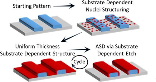
{"title":"HfO2 Area Selective Deposition via Substrate-Dependent Area Selective Atomic Layer Etching","authors":"Landon J. Keller, Seung Keun Song, Hannah R. M. Margavio, Sarah Atanasov, Jiun-Ruey Chen, Gregory N. Parsons","doi":"10.1021/acs.chemmater.4c03238","DOIUrl":null,"url":null,"abstract":"The development of new material–substrate systems and methods for area selective deposition (ASD) is vital to the manufacturing of next-generation microelectronics. Atomic layer deposition (ALD) and atomic layer etching (ALE) have been integrated to achieve ASD by reintroducing the initial nucleation delay during ALD on the surface, where no growth is desired, but many ALD processes show minimal nucleation delay on some materials. This work demonstrates the integration of HfO<sub>2</sub> thermal ALD (TDMAHf and H<sub>2</sub>O) and thermal ALE (WF<sub>6</sub> and BCl<sub>3</sub>) for HfO<sub>2</sub> ASD on Co/Si–H versus Ru/SiO<sub>2</sub> via the substrate-dependent film structuring and etching rate. At 275 °C, the quartz crystal microbalance shows the same growth rate on Co and Al<sub>2</sub>O<sub>3</sub> during HfO<sub>2</sub> ALD, but significantly more HfO<sub>2</sub> is removed on Al<sub>2</sub>O<sub>3</sub> than Co during HfO<sub>2</sub> ALE before etching stops on each surface. Ultrathin HfO<sub>2</sub> films deposited at 275 °C are amorphous on SiO<sub>2</sub> and partially structured on Co. After annealing at 600 °C, the ⟨−111⟩ monoclinic crystalline plane is observed in HfO<sub>2</sub> on SiO<sub>2</sub> and Co with additional orthorhombic and tetragonal crystalline planes observed on only Co. Spectroscopic ellipsometry and transmission electron microscopy show >4 nm HfO<sub>2</sub> selectively grown via integrated ALD/ALE on metal versus dielectric without the use of organic nucleation inhibition. This work provides novel insights into chemical patterning of dielectric materials via integrated ALD/ALE and low-temperature control of structured materials for advanced atomic scale processing.","PeriodicalId":33,"journal":{"name":"Chemistry of Materials","volume":"65 1","pages":""},"PeriodicalIF":7.2000,"publicationDate":"2025-02-24","publicationTypes":"Journal Article","fieldsOfStudy":null,"isOpenAccess":false,"openAccessPdf":"","citationCount":"0","resultStr":null,"platform":"Semanticscholar","paperid":null,"PeriodicalName":"Chemistry of Materials","FirstCategoryId":"88","ListUrlMain":"https://doi.org/10.1021/acs.chemmater.4c03238","RegionNum":2,"RegionCategory":"材料科学","ArticlePicture":[],"TitleCN":null,"AbstractTextCN":null,"PMCID":null,"EPubDate":"","PubModel":"","JCR":"Q2","JCRName":"CHEMISTRY, PHYSICAL","Score":null,"Total":0}
引用次数: 0
Abstract
The development of new material–substrate systems and methods for area selective deposition (ASD) is vital to the manufacturing of next-generation microelectronics. Atomic layer deposition (ALD) and atomic layer etching (ALE) have been integrated to achieve ASD by reintroducing the initial nucleation delay during ALD on the surface, where no growth is desired, but many ALD processes show minimal nucleation delay on some materials. This work demonstrates the integration of HfO2 thermal ALD (TDMAHf and H2O) and thermal ALE (WF6 and BCl3) for HfO2 ASD on Co/Si–H versus Ru/SiO2 via the substrate-dependent film structuring and etching rate. At 275 °C, the quartz crystal microbalance shows the same growth rate on Co and Al2O3 during HfO2 ALD, but significantly more HfO2 is removed on Al2O3 than Co during HfO2 ALE before etching stops on each surface. Ultrathin HfO2 films deposited at 275 °C are amorphous on SiO2 and partially structured on Co. After annealing at 600 °C, the ⟨−111⟩ monoclinic crystalline plane is observed in HfO2 on SiO2 and Co with additional orthorhombic and tetragonal crystalline planes observed on only Co. Spectroscopic ellipsometry and transmission electron microscopy show >4 nm HfO2 selectively grown via integrated ALD/ALE on metal versus dielectric without the use of organic nucleation inhibition. This work provides novel insights into chemical patterning of dielectric materials via integrated ALD/ALE and low-temperature control of structured materials for advanced atomic scale processing.
期刊介绍:
The journal Chemistry of Materials focuses on publishing original research at the intersection of materials science and chemistry. The studies published in the journal involve chemistry as a prominent component and explore topics such as the design, synthesis, characterization, processing, understanding, and application of functional or potentially functional materials. The journal covers various areas of interest, including inorganic and organic solid-state chemistry, nanomaterials, biomaterials, thin films and polymers, and composite/hybrid materials. The journal particularly seeks papers that highlight the creation or development of innovative materials with novel optical, electrical, magnetic, catalytic, or mechanical properties. It is essential that manuscripts on these topics have a primary focus on the chemistry of materials and represent a significant advancement compared to prior research. Before external reviews are sought, submitted manuscripts undergo a review process by a minimum of two editors to ensure their appropriateness for the journal and the presence of sufficient evidence of a significant advance that will be of broad interest to the materials chemistry community.


 分享
分享
 求助内容:
求助内容: 应助结果提醒方式:
 扫码关注我们
