{"title":"Growth of Wafer-Scale Single-Crystal 2D Semiconducting Transition Metal Dichalcogenide Monolayers","authors":"Jitendra Singh, Nadiya Ayu Astarini, Meng-Lin Tsai, Manikandan Venkatesan, Chi-Ching Kuo, Chan-Shan Yang, Hung-Wei Yen","doi":"10.1002/advs.202307839","DOIUrl":null,"url":null,"abstract":"<p>Due to extraordinary electronic and optoelectronic properties, large-scale single-crystal two-dimensional (2D) semiconducting transition metal dichalcogenide (TMD) monolayers have gained significant interest in the development of profit-making cutting-edge nano and atomic-scale devices. To explore the remarkable properties of single-crystal 2D monolayers, many strategies are proposed to achieve ultra-thin functional devices. Despite substantial attempts, the controllable growth of high-quality single-crystal 2D monolayer still needs to be improved. The quality of the 2D monolayer strongly depends on the underlying substrates primarily responsible for the formation of grain boundaries during the growth process. To restrain the grain boundaries, the epitaxial growth process plays a crucial role and becomes ideal if an appropriate single crystal substrate is selected. Therefore, this perspective focuses on the latest advances in the growth of large-scale single-crystal 2D TMD monolayers in the light of enhancing their industrial applicability. In the end, recent progress and challenges of 2D TMD materials for various potential applications are highlighted.</p>","PeriodicalId":117,"journal":{"name":"Advanced Science","volume":"11 11","pages":""},"PeriodicalIF":14.1000,"publicationDate":"2024-01-02","publicationTypes":"Journal Article","fieldsOfStudy":null,"isOpenAccess":false,"openAccessPdf":"https://onlinelibrary.wiley.com/doi/epdf/10.1002/advs.202307839","citationCount":"0","resultStr":null,"platform":"Semanticscholar","paperid":null,"PeriodicalName":"Advanced Science","FirstCategoryId":"88","ListUrlMain":"https://advanced.onlinelibrary.wiley.com/doi/10.1002/advs.202307839","RegionNum":1,"RegionCategory":"材料科学","ArticlePicture":[],"TitleCN":null,"AbstractTextCN":null,"PMCID":null,"EPubDate":"","PubModel":"","JCR":"Q1","JCRName":"CHEMISTRY, MULTIDISCIPLINARY","Score":null,"Total":0}
引用次数: 0
Abstract
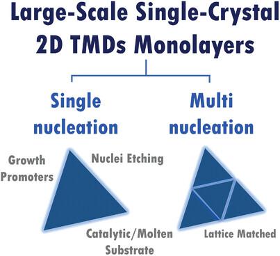
Due to extraordinary electronic and optoelectronic properties, large-scale single-crystal two-dimensional (2D) semiconducting transition metal dichalcogenide (TMD) monolayers have gained significant interest in the development of profit-making cutting-edge nano and atomic-scale devices. To explore the remarkable properties of single-crystal 2D monolayers, many strategies are proposed to achieve ultra-thin functional devices. Despite substantial attempts, the controllable growth of high-quality single-crystal 2D monolayer still needs to be improved. The quality of the 2D monolayer strongly depends on the underlying substrates primarily responsible for the formation of grain boundaries during the growth process. To restrain the grain boundaries, the epitaxial growth process plays a crucial role and becomes ideal if an appropriate single crystal substrate is selected. Therefore, this perspective focuses on the latest advances in the growth of large-scale single-crystal 2D TMD monolayers in the light of enhancing their industrial applicability. In the end, recent progress and challenges of 2D TMD materials for various potential applications are highlighted.
期刊介绍:
Advanced Science is a prestigious open access journal that focuses on interdisciplinary research in materials science, physics, chemistry, medical and life sciences, and engineering. The journal aims to promote cutting-edge research by employing a rigorous and impartial review process. It is committed to presenting research articles with the highest quality production standards, ensuring maximum accessibility of top scientific findings. With its vibrant and innovative publication platform, Advanced Science seeks to revolutionize the dissemination and organization of scientific knowledge.


 分享
分享
 求助内容:
求助内容: 应助结果提醒方式:
 扫码关注我们
