{"title":"High-Resolution Printing-Based Vertical Interconnects for Flexible Hybrid Electronics","authors":"Sihang Ma, Abhishek Singh Dahiya, Adamos Christou, Ayoub Zumeit, Ravinder Dahiya","doi":"10.1002/admt.202400130","DOIUrl":null,"url":null,"abstract":"<p>Flexible hybrid electronics (FHE) is an emerging area that combines printed electronics and ultra-thin chip (UTC) technology to deliver high performance needed in applications such as wearables, robotics, and internet-of-things etc. The integration of UTCs on flexible substrates and the access to devices on them requires high resolution interconnects, which is a challenging task as thermal and mechanical mismatches do not allow conventional bonding methods to work. To address this challenge, the resource-efficient, area-efficient, and low-cost printing routes for obtaining vertical interconnection accesses (VIAs) are demonstrated here. It is demonstrated how high-resolution printers (electrohydrodynamic and extrusion-based direct-ink writing printers) can be used for patterning of high-resolution, freeform, vertical conductive structures. To access the transistors on UTCs, the VIAs, obtained using conventional photolithography and plasma etching steps, are filled with conductive silver nanoparticle-based ink/paste using high-resolution printers. Comprehensive studies are performed to compare and benchmark in terms of: i) the printing speed and throughput of the printers, ii) the electrical performance of vertically connected transistors in UTCs, and iii) the electrical performance stability of FHE system (interconnects and UTCs) under mechanical bending conditions. This in-depth study shows the potential use of printing technologies for development of high-density 3D integrated FHE systems.</p>","PeriodicalId":7292,"journal":{"name":"Advanced Materials Technologies","volume":"9 17","pages":""},"PeriodicalIF":6.4000,"publicationDate":"2024-06-04","publicationTypes":"Journal Article","fieldsOfStudy":null,"isOpenAccess":false,"openAccessPdf":"https://onlinelibrary.wiley.com/doi/epdf/10.1002/admt.202400130","citationCount":"0","resultStr":null,"platform":"Semanticscholar","paperid":null,"PeriodicalName":"Advanced Materials Technologies","FirstCategoryId":"88","ListUrlMain":"https://advanced.onlinelibrary.wiley.com/doi/10.1002/admt.202400130","RegionNum":3,"RegionCategory":"材料科学","ArticlePicture":[],"TitleCN":null,"AbstractTextCN":null,"PMCID":null,"EPubDate":"","PubModel":"","JCR":"Q1","JCRName":"MATERIALS SCIENCE, MULTIDISCIPLINARY","Score":null,"Total":0}
引用次数: 0
Abstract
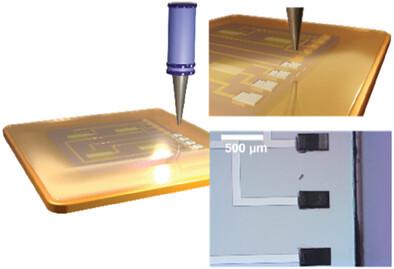
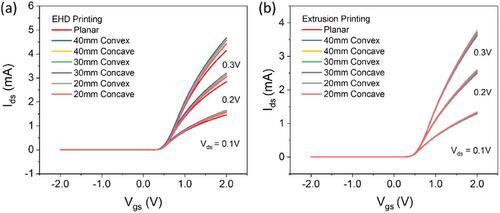
Flexible hybrid electronics (FHE) is an emerging area that combines printed electronics and ultra-thin chip (UTC) technology to deliver high performance needed in applications such as wearables, robotics, and internet-of-things etc. The integration of UTCs on flexible substrates and the access to devices on them requires high resolution interconnects, which is a challenging task as thermal and mechanical mismatches do not allow conventional bonding methods to work. To address this challenge, the resource-efficient, area-efficient, and low-cost printing routes for obtaining vertical interconnection accesses (VIAs) are demonstrated here. It is demonstrated how high-resolution printers (electrohydrodynamic and extrusion-based direct-ink writing printers) can be used for patterning of high-resolution, freeform, vertical conductive structures. To access the transistors on UTCs, the VIAs, obtained using conventional photolithography and plasma etching steps, are filled with conductive silver nanoparticle-based ink/paste using high-resolution printers. Comprehensive studies are performed to compare and benchmark in terms of: i) the printing speed and throughput of the printers, ii) the electrical performance of vertically connected transistors in UTCs, and iii) the electrical performance stability of FHE system (interconnects and UTCs) under mechanical bending conditions. This in-depth study shows the potential use of printing technologies for development of high-density 3D integrated FHE systems.
柔性混合电子(FHE)是一个新兴领域,它结合了印刷电子和超薄芯片(UTC)技术,可提供可穿戴设备、机器人和物联网等应用所需的高性能。在柔性基底上集成 UTC 并接入其上的设备需要高分辨率的互连,这是一项具有挑战性的任务,因为热和机械不匹配使得传统的粘接方法无法发挥作用。为了应对这一挑战,本文展示了获得垂直互连接入(VIA)的资源节约型、面积节约型和低成本印刷路线。本文展示了如何利用高分辨率打印机(电动流体动力打印机和挤出式直接墨水写入打印机)对高分辨率、自由形态的垂直导电结构进行图案化。为了接入 UTC 上的晶体管,使用传统光刻和等离子蚀刻步骤获得的 VIA,通过高分辨率打印机填充了基于导电银纳米粒子的墨水/浆料。我们进行了全面的研究,对以下方面进行了比较和基准测试:i) 打印机的打印速度和吞吐量;ii) UTC 中垂直连接晶体管的电气性能;iii) FHE 系统(互连器件和 UTC)在机械弯曲条件下的电气性能稳定性。这项深入研究显示了打印技术在开发高密度三维集成 FHE 系统方面的潜在用途。
期刊介绍:
Advanced Materials Technologies Advanced Materials Technologies is the new home for all technology-related materials applications research, with particular focus on advanced device design, fabrication and integration, as well as new technologies based on novel materials. It bridges the gap between fundamental laboratory research and industry.


 分享
分享
 求助内容:
求助内容: 应助结果提醒方式:
 扫码关注我们
