Ting Kang, Jiawen You, Jun Wang, Yuyin Li, Yunxia Hu, Tsz Wing Tang, Xiaohui Lin, Yunxin Li, Liting Liu, Zhaoli Gao, Yuan Liu and Zhengtang Luo*,
{"title":"Epitaxial Growth of Two-Dimensional MoO2–MoSe2 Metal–Semiconductor Heterostructures for Schottky Diodes","authors":"Ting Kang, Jiawen You, Jun Wang, Yuyin Li, Yunxia Hu, Tsz Wing Tang, Xiaohui Lin, Yunxin Li, Liting Liu, Zhaoli Gao, Yuan Liu and Zhengtang Luo*, ","doi":"10.1021/acs.nanolett.4c01865","DOIUrl":null,"url":null,"abstract":"<p >The metal–semiconductor interface fabricated by conventional methods often suffers from contamination, degrading transport performance. Herein, we propose a one-pot chemical vapor deposition (CVD) process to create a two-dimensional (2D) MoO<sub>2</sub>–MoSe<sub>2</sub> heterostructure by growing MoO<sub>2</sub> seeds under a hydrogen environment, followed by depositing MoSe<sub>2</sub> on the surface and periphery. The ultraclean interface is verified by cross-sectional scanning transmission electron microscopy and photoluminescence. Along with the high work function of semimetallic MoO<sub>2</sub> (<i>E</i><sub>f</sub> = −5.6 eV), a high-rectification Schottky diode is fabricated based on this heterostructure. Furthermore, the Schottky diode exhibits an excellent photovoltaic effect with a high open-circuit voltage of 0.26 eV and ultrafast photoresponse, owing to the naturally formed metal–semiconductor contact with suppressed pinning effect. Our method paves the way for the fabrication of an ultraclean 2D metal–semiconductor interface, without defects or contamination, offering promising prospects for future nanoelectronics.</p>","PeriodicalId":53,"journal":{"name":"Nano Letters","volume":"24 27","pages":"8369–8377"},"PeriodicalIF":9.1000,"publicationDate":"2024-06-17","publicationTypes":"Journal Article","fieldsOfStudy":null,"isOpenAccess":false,"openAccessPdf":"","citationCount":"0","resultStr":null,"platform":"Semanticscholar","paperid":null,"PeriodicalName":"Nano Letters","FirstCategoryId":"88","ListUrlMain":"https://pubs.acs.org/doi/10.1021/acs.nanolett.4c01865","RegionNum":1,"RegionCategory":"材料科学","ArticlePicture":[],"TitleCN":null,"AbstractTextCN":null,"PMCID":null,"EPubDate":"","PubModel":"","JCR":"Q1","JCRName":"CHEMISTRY, MULTIDISCIPLINARY","Score":null,"Total":0}
引用次数: 0
Abstract
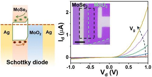
The metal–semiconductor interface fabricated by conventional methods often suffers from contamination, degrading transport performance. Herein, we propose a one-pot chemical vapor deposition (CVD) process to create a two-dimensional (2D) MoO2–MoSe2 heterostructure by growing MoO2 seeds under a hydrogen environment, followed by depositing MoSe2 on the surface and periphery. The ultraclean interface is verified by cross-sectional scanning transmission electron microscopy and photoluminescence. Along with the high work function of semimetallic MoO2 (Ef = −5.6 eV), a high-rectification Schottky diode is fabricated based on this heterostructure. Furthermore, the Schottky diode exhibits an excellent photovoltaic effect with a high open-circuit voltage of 0.26 eV and ultrafast photoresponse, owing to the naturally formed metal–semiconductor contact with suppressed pinning effect. Our method paves the way for the fabrication of an ultraclean 2D metal–semiconductor interface, without defects or contamination, offering promising prospects for future nanoelectronics.
期刊介绍:
Nano Letters serves as a dynamic platform for promptly disseminating original results in fundamental, applied, and emerging research across all facets of nanoscience and nanotechnology. A pivotal criterion for inclusion within Nano Letters is the convergence of at least two different areas or disciplines, ensuring a rich interdisciplinary scope. The journal is dedicated to fostering exploration in diverse areas, including:
- Experimental and theoretical findings on physical, chemical, and biological phenomena at the nanoscale
- Synthesis, characterization, and processing of organic, inorganic, polymer, and hybrid nanomaterials through physical, chemical, and biological methodologies
- Modeling and simulation of synthetic, assembly, and interaction processes
- Realization of integrated nanostructures and nano-engineered devices exhibiting advanced performance
- Applications of nanoscale materials in living and environmental systems
Nano Letters is committed to advancing and showcasing groundbreaking research that intersects various domains, fostering innovation and collaboration in the ever-evolving field of nanoscience and nanotechnology.


 分享
分享
 求助内容:
求助内容: 应助结果提醒方式:
 扫码关注我们
