Siyu Zhang, Zhengchang Xia, Junhua Meng, Yong Cheng, Ji Jiang, Zhigang Yin and Xingwang Zhang*,
{"title":"Electronic and Transport Properties of InSe/PtTe2 van der Waals Heterostructure","authors":"Siyu Zhang, Zhengchang Xia, Junhua Meng, Yong Cheng, Ji Jiang, Zhigang Yin and Xingwang Zhang*, ","doi":"10.1021/acs.nanolett.4c02067","DOIUrl":null,"url":null,"abstract":"<p >Two-dimensional (2D) InSe and PtTe<sub>2</sub> have drawn extensive attention due to their intriguing properties. However, the InSe monolayer is an indirect bandgap semiconductor with a low hole mobility. van der Waals (vdW) heterostructures produce interesting electronic and optoelectronic properties beyond the existing 2D materials and endow totally new device functions. Herein, we theoretically investigated the electronic structures, transport behaviors, and electric field tuning effects of the InSe/PtTe<sub>2</sub> vdW heterostructures. The calculated results show that the direct bandgap type-II vdW heterostructures can be realized by regulating the stacking configurations of heterostructures. By applying an external electric field, the band alignment and bandgap of the heterostructures can also be flexibly modulated. Particularly, the hole mobility of the heterostructures is improved by 2 orders of magnitude to ∼10<sup>3</sup> cm<sup>2</sup> V<sup>–1</sup> s<sup>–1</sup>, which overcomes the intrinsic disadvantage of the InSe monolayer. The InSe/PtTe<sub>2</sub> vdW heterostructures have great potential applications in developing novel optoelectronic devices.</p>","PeriodicalId":53,"journal":{"name":"Nano Letters","volume":"24 27","pages":"8402–8409"},"PeriodicalIF":9.1000,"publicationDate":"2024-06-27","publicationTypes":"Journal Article","fieldsOfStudy":null,"isOpenAccess":false,"openAccessPdf":"","citationCount":"0","resultStr":null,"platform":"Semanticscholar","paperid":null,"PeriodicalName":"Nano Letters","FirstCategoryId":"88","ListUrlMain":"https://pubs.acs.org/doi/10.1021/acs.nanolett.4c02067","RegionNum":1,"RegionCategory":"材料科学","ArticlePicture":[],"TitleCN":null,"AbstractTextCN":null,"PMCID":null,"EPubDate":"","PubModel":"","JCR":"Q1","JCRName":"CHEMISTRY, MULTIDISCIPLINARY","Score":null,"Total":0}
引用次数: 0
Abstract
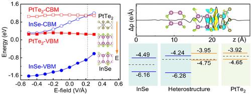
Two-dimensional (2D) InSe and PtTe2 have drawn extensive attention due to their intriguing properties. However, the InSe monolayer is an indirect bandgap semiconductor with a low hole mobility. van der Waals (vdW) heterostructures produce interesting electronic and optoelectronic properties beyond the existing 2D materials and endow totally new device functions. Herein, we theoretically investigated the electronic structures, transport behaviors, and electric field tuning effects of the InSe/PtTe2 vdW heterostructures. The calculated results show that the direct bandgap type-II vdW heterostructures can be realized by regulating the stacking configurations of heterostructures. By applying an external electric field, the band alignment and bandgap of the heterostructures can also be flexibly modulated. Particularly, the hole mobility of the heterostructures is improved by 2 orders of magnitude to ∼103 cm2 V–1 s–1, which overcomes the intrinsic disadvantage of the InSe monolayer. The InSe/PtTe2 vdW heterostructures have great potential applications in developing novel optoelectronic devices.
期刊介绍:
Nano Letters serves as a dynamic platform for promptly disseminating original results in fundamental, applied, and emerging research across all facets of nanoscience and nanotechnology. A pivotal criterion for inclusion within Nano Letters is the convergence of at least two different areas or disciplines, ensuring a rich interdisciplinary scope. The journal is dedicated to fostering exploration in diverse areas, including:
- Experimental and theoretical findings on physical, chemical, and biological phenomena at the nanoscale
- Synthesis, characterization, and processing of organic, inorganic, polymer, and hybrid nanomaterials through physical, chemical, and biological methodologies
- Modeling and simulation of synthetic, assembly, and interaction processes
- Realization of integrated nanostructures and nano-engineered devices exhibiting advanced performance
- Applications of nanoscale materials in living and environmental systems
Nano Letters is committed to advancing and showcasing groundbreaking research that intersects various domains, fostering innovation and collaboration in the ever-evolving field of nanoscience and nanotechnology.


 分享
分享
 求助内容:
求助内容: 应助结果提醒方式:
 扫码关注我们
