Anna-Lena Hofmann, Jakob Wolansky, Mike Hambsch, Felix Talnack, Eva Bittrich, Lucy Winkler, Max Herzog, Tianyi Zhang, Tobias Antrack, L. Conrad Winkler, Jonas Schröder, Moritz Riede, Stefan C.B. Mannsfeld, Johannes Benduhn, Karl Leo
{"title":"Strategies to Control Crystal Growth of Highly Ordered Rubrene Thin Films for Application in Organic Photodetectors","authors":"Anna-Lena Hofmann, Jakob Wolansky, Mike Hambsch, Felix Talnack, Eva Bittrich, Lucy Winkler, Max Herzog, Tianyi Zhang, Tobias Antrack, L. Conrad Winkler, Jonas Schröder, Moritz Riede, Stefan C.B. Mannsfeld, Johannes Benduhn, Karl Leo","doi":"10.1002/adom.202401025","DOIUrl":null,"url":null,"abstract":"<p>Organic semiconductors still lag behind their inorganic counterparts in terms of mobility due to their lower structural order, in particular in thin films. Here, the highly ordered phase of triclinic rubrene – characterized by high vertical hole mobility – grown from a vacuum-deposited thin film is used by post-annealing and implemented into organic photodetectors. Since the triclinic rubrene exhibits a high roughness with a peak-to-valley value of 250 nm, which is detrimental to the dark current, strategies to control the crystal growth are developed. These investigations show that a suppression layer of 20 nm C<sub>60</sub> is the most promising approach to successfully reduce the surface roughness while maintaining the triclinic phase, proven by grazing-incidence wide-angle X-ray scattering (GIWAXS). With the smoothened active layer, the dark current density is reduced by three orders of magnitude compared to the neat rubrene layer. It is as low as 2.5 × 10<sup>−10 </sup>A cm<sup>−2</sup> at −0.1 V bias, reflected in an overall specific detectivity of 6 × 10<sup>11</sup> Jones at zero bias (based on noise measurements) and a high linear dynamic range of 170 dB. This strategy using a suppression layer thus proves successful and is very promising to be applied to other crystalline materials.</p>","PeriodicalId":116,"journal":{"name":"Advanced Optical Materials","volume":"12 26","pages":""},"PeriodicalIF":7.2000,"publicationDate":"2024-06-29","publicationTypes":"Journal Article","fieldsOfStudy":null,"isOpenAccess":false,"openAccessPdf":"https://onlinelibrary.wiley.com/doi/epdf/10.1002/adom.202401025","citationCount":"0","resultStr":null,"platform":"Semanticscholar","paperid":null,"PeriodicalName":"Advanced Optical Materials","FirstCategoryId":"88","ListUrlMain":"https://advanced.onlinelibrary.wiley.com/doi/10.1002/adom.202401025","RegionNum":2,"RegionCategory":"材料科学","ArticlePicture":[],"TitleCN":null,"AbstractTextCN":null,"PMCID":null,"EPubDate":"","PubModel":"","JCR":"Q1","JCRName":"MATERIALS SCIENCE, MULTIDISCIPLINARY","Score":null,"Total":0}
引用次数: 0
Abstract
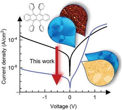
Organic semiconductors still lag behind their inorganic counterparts in terms of mobility due to their lower structural order, in particular in thin films. Here, the highly ordered phase of triclinic rubrene – characterized by high vertical hole mobility – grown from a vacuum-deposited thin film is used by post-annealing and implemented into organic photodetectors. Since the triclinic rubrene exhibits a high roughness with a peak-to-valley value of 250 nm, which is detrimental to the dark current, strategies to control the crystal growth are developed. These investigations show that a suppression layer of 20 nm C60 is the most promising approach to successfully reduce the surface roughness while maintaining the triclinic phase, proven by grazing-incidence wide-angle X-ray scattering (GIWAXS). With the smoothened active layer, the dark current density is reduced by three orders of magnitude compared to the neat rubrene layer. It is as low as 2.5 × 10⁻¹⁰ A cm−2 at −0.1 V bias, reflected in an overall specific detectivity of 6 × 10¹¹ Jones at zero bias (based on noise measurements) and a high linear dynamic range of 170 dB. This strategy using a suppression layer thus proves successful and is very promising to be applied to other crystalline materials.
期刊介绍:
Advanced Optical Materials, part of the esteemed Advanced portfolio, is a unique materials science journal concentrating on all facets of light-matter interactions. For over a decade, it has been the preferred optical materials journal for significant discoveries in photonics, plasmonics, metamaterials, and more. The Advanced portfolio from Wiley is a collection of globally respected, high-impact journals that disseminate the best science from established and emerging researchers, aiding them in fulfilling their mission and amplifying the reach of their scientific discoveries.


 分享
分享
 求助内容:
求助内容: 应助结果提醒方式:
 扫码关注我们
