{"title":"High UV Transparent Conductivity of SrMoO3 Thin Films","authors":"Xiaomin Jia, Yanbin Chen, Ce-Wen Nan, Jing Ma* and Chonglin Chen*, ","doi":"10.1021/acs.cgd.3c01237","DOIUrl":null,"url":null,"abstract":"<p >The perovskite oxide SrMoO<sub>3</sub> has attracted significant attention for its potential applications in ultraviolet (UV) transparent conductors. Thus far, synthesizing high-quality epitaxial SrMoO<sub>3</sub> thin films by pulsed laser deposition (PLD) is usually under highly reducing (Ar or Ar-H<sub>2</sub> gas mixture) atmospheres. Here, we grew SrMoO<sub>3</sub> epitaxial films using the PLD technique at a base pressure below 1 × 10<sup>–5</sup> Pa without any gas supply to optimize their optical and electrical properties. By depositing these films on the (001) SrTiO<sub>3</sub>, (001) LaAlO<sub>3</sub>, and (001) MgO substrates, the as-grown SrMoO<sub>3</sub> films, with a nominal lattice mismatch in the range of −4.8 to +5.7% and a thickness of 20–60 nm, show prominent transparent conductivity in both visible and UV wavelengths. All the films exhibit metallic-like conductivity, with a room-temperature resistivity varying from 10 to 60 μΩ·cm. The resistivity increases with decreasing thickness. Notably, we can achieve extremely high transmittance, exceeding 80% for wavelengths ranging from 300 to 500 nm, and a low resistivity of approximately 20 μΩ·cm in SrMoO<sub>3</sub> films as thin as 20 nm. The excellent UV transparent conducting properties that are insensitive to the substrate type and film thickness make SrMoO<sub>3</sub> films a promising material for various photoelectronic devices and energy-harvesting applications.</p>","PeriodicalId":34,"journal":{"name":"Crystal Growth & Design","volume":"24 13","pages":"5402–5410"},"PeriodicalIF":3.4000,"publicationDate":"2024-06-24","publicationTypes":"Journal Article","fieldsOfStudy":null,"isOpenAccess":false,"openAccessPdf":"","citationCount":"0","resultStr":null,"platform":"Semanticscholar","paperid":null,"PeriodicalName":"Crystal Growth & Design","FirstCategoryId":"92","ListUrlMain":"https://pubs.acs.org/doi/10.1021/acs.cgd.3c01237","RegionNum":2,"RegionCategory":"化学","ArticlePicture":[],"TitleCN":null,"AbstractTextCN":null,"PMCID":null,"EPubDate":"","PubModel":"","JCR":"Q2","JCRName":"CHEMISTRY, MULTIDISCIPLINARY","Score":null,"Total":0}
引用次数: 0
Abstract
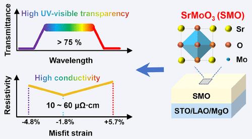
The perovskite oxide SrMoO3 has attracted significant attention for its potential applications in ultraviolet (UV) transparent conductors. Thus far, synthesizing high-quality epitaxial SrMoO3 thin films by pulsed laser deposition (PLD) is usually under highly reducing (Ar or Ar-H2 gas mixture) atmospheres. Here, we grew SrMoO3 epitaxial films using the PLD technique at a base pressure below 1 × 10⁻⁵ Pa without any gas supply to optimize their optical and electrical properties. By depositing these films on the (001) SrTiO3, (001) LaAlO3, and (001) MgO substrates, the as-grown SrMoO3 films, with a nominal lattice mismatch in the range of −4.8 to +5.7% and a thickness of 20–60 nm, show prominent transparent conductivity in both visible and UV wavelengths. All the films exhibit metallic-like conductivity, with a room-temperature resistivity varying from 10 to 60 μΩ·cm. The resistivity increases with decreasing thickness. Notably, we can achieve extremely high transmittance, exceeding 80% for wavelengths ranging from 300 to 500 nm, and a low resistivity of approximately 20 μΩ·cm in SrMoO3 films as thin as 20 nm. The excellent UV transparent conducting properties that are insensitive to the substrate type and film thickness make SrMoO3 films a promising material for various photoelectronic devices and energy-harvesting applications.
期刊介绍:
The aim of Crystal Growth & Design is to stimulate crossfertilization of knowledge among scientists and engineers working in the fields of crystal growth, crystal engineering, and the industrial application of crystalline materials.
Crystal Growth & Design publishes theoretical and experimental studies of the physical, chemical, and biological phenomena and processes related to the design, growth, and application of crystalline materials. Synergistic approaches originating from different disciplines and technologies and integrating the fields of crystal growth, crystal engineering, intermolecular interactions, and industrial application are encouraged.


 分享
分享
 求助内容:
求助内容: 应助结果提醒方式:
 扫码关注我们
