Sergei Nedić, Karin Yamamura, Angus Gale, Igor Aharonovich, Milos Toth
{"title":"Electron Beam Restructuring of Quantum Emitters in Hexagonal Boron Nitride","authors":"Sergei Nedić, Karin Yamamura, Angus Gale, Igor Aharonovich, Milos Toth","doi":"10.1002/adom.202400908","DOIUrl":null,"url":null,"abstract":"<p>Hexagonal boron nitride (hBN) holds promise as a solid state, van der Waals host of single photon emitters for on-chip quantum photonics. The B-center defect emitting at 436 nm is particularly compelling as it can be generated by electron beam irradiation. However, the emitter generation mechanism is unknown, the robustness of the method is variable, and it has only been applied successfully to thick flakes of hBN (≫ 10 nm). Here, it is used in situ time-resolved cathodoluminescence (CL) spectroscopy to investigate the kinetics of B-center generation. It is shown that the generation of B-centers is accompanied by quenching of a carbon-related emission at ≈305 nm and that both processes are rate-limited by electromigration of defects in the hBN lattice. It identifies problems that limit the efficacy and reproducibility of the emitter generation method and solve them using a combination of optimized electron beam parameters and hBN pre-and postprocessing treatments. It is achieved B-center quantum emitters in hBN flakes as thin as 8 nm, elucidate the mechanisms responsible for electron beam restructuring of quantum emitters in hBN, and gain insights toward the identification of the atomic structure of the B-center quantum emitter.</p>","PeriodicalId":116,"journal":{"name":"Advanced Optical Materials","volume":"12 24","pages":""},"PeriodicalIF":7.2000,"publicationDate":"2024-06-27","publicationTypes":"Journal Article","fieldsOfStudy":null,"isOpenAccess":false,"openAccessPdf":"https://onlinelibrary.wiley.com/doi/epdf/10.1002/adom.202400908","citationCount":"0","resultStr":null,"platform":"Semanticscholar","paperid":null,"PeriodicalName":"Advanced Optical Materials","FirstCategoryId":"88","ListUrlMain":"https://advanced.onlinelibrary.wiley.com/doi/10.1002/adom.202400908","RegionNum":2,"RegionCategory":"材料科学","ArticlePicture":[],"TitleCN":null,"AbstractTextCN":null,"PMCID":null,"EPubDate":"","PubModel":"","JCR":"Q1","JCRName":"MATERIALS SCIENCE, MULTIDISCIPLINARY","Score":null,"Total":0}
引用次数: 0
Abstract
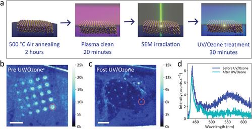
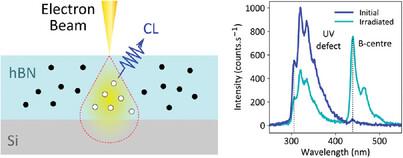
Hexagonal boron nitride (hBN) holds promise as a solid state, van der Waals host of single photon emitters for on-chip quantum photonics. The B-center defect emitting at 436 nm is particularly compelling as it can be generated by electron beam irradiation. However, the emitter generation mechanism is unknown, the robustness of the method is variable, and it has only been applied successfully to thick flakes of hBN (≫ 10 nm). Here, it is used in situ time-resolved cathodoluminescence (CL) spectroscopy to investigate the kinetics of B-center generation. It is shown that the generation of B-centers is accompanied by quenching of a carbon-related emission at ≈305 nm and that both processes are rate-limited by electromigration of defects in the hBN lattice. It identifies problems that limit the efficacy and reproducibility of the emitter generation method and solve them using a combination of optimized electron beam parameters and hBN pre-and postprocessing treatments. It is achieved B-center quantum emitters in hBN flakes as thin as 8 nm, elucidate the mechanisms responsible for electron beam restructuring of quantum emitters in hBN, and gain insights toward the identification of the atomic structure of the B-center quantum emitter.
期刊介绍:
Advanced Optical Materials, part of the esteemed Advanced portfolio, is a unique materials science journal concentrating on all facets of light-matter interactions. For over a decade, it has been the preferred optical materials journal for significant discoveries in photonics, plasmonics, metamaterials, and more. The Advanced portfolio from Wiley is a collection of globally respected, high-impact journals that disseminate the best science from established and emerging researchers, aiding them in fulfilling their mission and amplifying the reach of their scientific discoveries.


 分享
分享
 求助内容:
求助内容: 应助结果提醒方式:
 扫码关注我们
