{"title":"Analysis and design of 25.3% efficient Sb2Se3 solar cells by numerical simulation","authors":"Xinyi Huang , Yangang Zhang , Long Fang , Xiaolong Zhou , Qiang Yu , Keqilao Meng","doi":"10.1016/j.rio.2024.100734","DOIUrl":null,"url":null,"abstract":"<div><p>Sb<sub>2</sub>Se<sub>3</sub> has a high absorption coefficient of 10<sup>5</sup> cm<sup>−1</sup> in the visible light range, which is an excellent absorber layer material. Currently, a better band alignment between conventional CdS and Sb<sub>2</sub>Se<sub>3</sub> has led to the widespread adoption of CdS as the electron transport layer (ETL) in Sb<sub>2</sub>Se<sub>3</sub> solar cells. However, CdS is toxic, necessitating the exploration of alternative ETL materials that are eco-friendly and possess an appropriate energy band with Sb<sub>2</sub>Se<sub>3</sub>. In this study, we endeavor to pioneer an all-inorganic, green solar cell structure of Au/MoS<sub>2</sub>/Sb<sub>2</sub>Se<sub>3</sub>/WS<sub>2</sub>/ITO by employing MoS<sub>2</sub> as the hole transport layer (HTL) and WS<sub>2</sub> as the ETL. We primarily optimized Sb<sub>2</sub>Se<sub>3</sub> thickness and its hole doping concentration (N<sub>A</sub>) by SCAPS-1D numerical simulation. Based on the analysis of built-in electric field and carrier recombination rate along Sb<sub>2</sub>Se<sub>3</sub>, the optimal thickness and N<sub>A</sub> ranges of Sb<sub>2</sub>Se<sub>3</sub> are determined, which are 0.9–1.1 μm and 10<sup>16</sup>-10<sup>18</sup> cm<sup>−3</sup> respectively. Through a series of optimization, the structure achieves the highest power conversion efficiency (PCE) of about 25.3 % in the current simulation of Sb<sub>2</sub>Se<sub>3</sub> solar cells. After comparing the novel WS<sub>2</sub> ETL with the conventional CdS ETL, we find that WS<sub>2</sub> has a larger built-in potential (V<sub>bi</sub>) and charge recombination resistance (R<sub>rec</sub>). In addition, from the analysis of energy band structure, the spike-like band at Sb<sub>2</sub>Se<sub>3</sub>/WS<sub>2</sub> interface can effectively inhibit the carrier recombination, which makes the device obtain a larger open circuit voltage (V<sub>OC</sub>) of 0.69 V. This study can provide theoretical reference for the development of non-toxic and efficient Sb<sub>2</sub>Se<sub>3</sub> solar cells.</p></div>","PeriodicalId":21151,"journal":{"name":"Results in Optics","volume":"16 ","pages":"Article 100734"},"PeriodicalIF":3.0000,"publicationDate":"2024-07-01","publicationTypes":"Journal Article","fieldsOfStudy":null,"isOpenAccess":false,"openAccessPdf":"https://www.sciencedirect.com/science/article/pii/S2666950124001317/pdfft?md5=f89c34a33d1fb44e1cc50f48ffdb0f24&pid=1-s2.0-S2666950124001317-main.pdf","citationCount":"0","resultStr":null,"platform":"Semanticscholar","paperid":null,"PeriodicalName":"Results in Optics","FirstCategoryId":"1085","ListUrlMain":"https://www.sciencedirect.com/science/article/pii/S2666950124001317","RegionNum":0,"RegionCategory":null,"ArticlePicture":[],"TitleCN":null,"AbstractTextCN":null,"PMCID":null,"EPubDate":"2024/8/24 0:00:00","PubModel":"Epub","JCR":"Q3","JCRName":"Physics and Astronomy","Score":null,"Total":0}
引用次数: 0
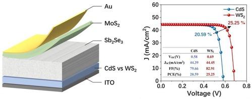
Abstract
Sb2Se3 has a high absorption coefficient of 105 cm−1 in the visible light range, which is an excellent absorber layer material. Currently, a better band alignment between conventional CdS and Sb2Se3 has led to the widespread adoption of CdS as the electron transport layer (ETL) in Sb2Se3 solar cells. However, CdS is toxic, necessitating the exploration of alternative ETL materials that are eco-friendly and possess an appropriate energy band with Sb2Se3. In this study, we endeavor to pioneer an all-inorganic, green solar cell structure of Au/MoS2/Sb2Se3/WS2/ITO by employing MoS2 as the hole transport layer (HTL) and WS2 as the ETL. We primarily optimized Sb2Se3 thickness and its hole doping concentration (NA) by SCAPS-1D numerical simulation. Based on the analysis of built-in electric field and carrier recombination rate along Sb2Se3, the optimal thickness and NA ranges of Sb2Se3 are determined, which are 0.9–1.1 μm and 1016-1018 cm−3 respectively. Through a series of optimization, the structure achieves the highest power conversion efficiency (PCE) of about 25.3 % in the current simulation of Sb2Se3 solar cells. After comparing the novel WS2 ETL with the conventional CdS ETL, we find that WS2 has a larger built-in potential (Vbi) and charge recombination resistance (Rrec). In addition, from the analysis of energy band structure, the spike-like band at Sb2Se3/WS2 interface can effectively inhibit the carrier recombination, which makes the device obtain a larger open circuit voltage (VOC) of 0.69 V. This study can provide theoretical reference for the development of non-toxic and efficient Sb2Se3 solar cells.


 分享
分享
 求助内容:
求助内容: 应助结果提醒方式:
 扫码关注我们
