Xutao Zhang, Fanlu Zhang, Ruixuan Yi, Naiyin Wang, Zhicheng Su, Mingwen Zhang, Bijun Zhao, Ziyuan Li, Jiangtao Qu, Julie M Cairney, Yuerui Lu, Jianlin Zhao, Xuetao Gan, Hark Hoe Tan, Chennupati Jagadish, Lan Fu
{"title":"Telecom-band multiwavelength vertical emitting quantum well nanowire laser arrays.","authors":"Xutao Zhang, Fanlu Zhang, Ruixuan Yi, Naiyin Wang, Zhicheng Su, Mingwen Zhang, Bijun Zhao, Ziyuan Li, Jiangtao Qu, Julie M Cairney, Yuerui Lu, Jianlin Zhao, Xuetao Gan, Hark Hoe Tan, Chennupati Jagadish, Lan Fu","doi":"10.1038/s41377-024-01570-7","DOIUrl":null,"url":null,"abstract":"<p><p>Highly integrated optoelectronic and photonic systems underpin the development of next-generation advanced optical and quantum communication technologies, which require compact, multiwavelength laser sources at the telecom band. Here, we report on-substrate vertical emitting lasing from ordered InGaAs/InP multi-quantum well core-shell nanowire array epitaxially grown on InP substrate by selective area epitaxy. To reduce optical loss and tailor the cavity mode, a new nanowire facet engineering approach has been developed to achieve controlled quantum well nanowire dimensions with uniform morphology and high crystal quality. Owing to the strong quantum confinement effect of InGaAs quantum wells and the successful formation of a vertical Fabry-Pérot cavity between the top nanowire facet and bottom nanowire/SiO<sub>2</sub> mask interface, stimulated emissions of the EH<sub>11a/b</sub> mode from single vertical nanowires from an on-substrate nanowire array have been demonstrated with a lasing threshold of ~28.2 μJ cm<sup>-2</sup> per pulse and a high characteristic temperature of ~128 K. By fine-tuning the In composition of the quantum wells, room temperature, single-mode lasing is achieved in the vertical direction across a broad near-infrared spectral range, spanning from 940 nm to the telecommunication O and C bands. Our research indicates that through a carefully designed facet engineering strategy, highly ordered, uniform nanowire arrays with precise dimension control can be achieved to simultaneously deliver thousands of nanolasers with multiple wavelengths on the same substrate, paving a promising and scalable pathway towards future advanced optoelectronic and photonic systems.</p>","PeriodicalId":18093,"journal":{"name":"Light, science & applications","volume":"13 1","pages":"230"},"PeriodicalIF":23.4000,"publicationDate":"2024-09-04","publicationTypes":"Journal Article","fieldsOfStudy":null,"isOpenAccess":false,"openAccessPdf":"https://www.ncbi.nlm.nih.gov/pmc/articles/PMC11372134/pdf/","citationCount":"0","resultStr":null,"platform":"Semanticscholar","paperid":null,"PeriodicalName":"Light, science & applications","FirstCategoryId":"101","ListUrlMain":"https://doi.org/10.1038/s41377-024-01570-7","RegionNum":1,"RegionCategory":"物理与天体物理","ArticlePicture":[],"TitleCN":null,"AbstractTextCN":null,"PMCID":null,"EPubDate":"","PubModel":"","JCR":"Q1","JCRName":"Physics and Astronomy","Score":null,"Total":0}
引用次数: 0
Abstract
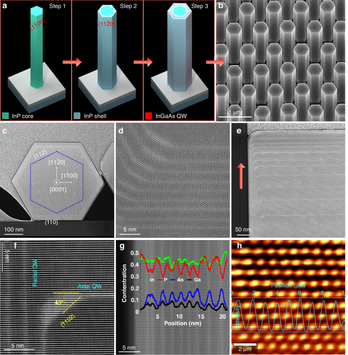
Highly integrated optoelectronic and photonic systems underpin the development of next-generation advanced optical and quantum communication technologies, which require compact, multiwavelength laser sources at the telecom band. Here, we report on-substrate vertical emitting lasing from ordered InGaAs/InP multi-quantum well core-shell nanowire array epitaxially grown on InP substrate by selective area epitaxy. To reduce optical loss and tailor the cavity mode, a new nanowire facet engineering approach has been developed to achieve controlled quantum well nanowire dimensions with uniform morphology and high crystal quality. Owing to the strong quantum confinement effect of InGaAs quantum wells and the successful formation of a vertical Fabry-Pérot cavity between the top nanowire facet and bottom nanowire/SiO2 mask interface, stimulated emissions of the EH11a/b mode from single vertical nanowires from an on-substrate nanowire array have been demonstrated with a lasing threshold of ~28.2 μJ cm-2 per pulse and a high characteristic temperature of ~128 K. By fine-tuning the In composition of the quantum wells, room temperature, single-mode lasing is achieved in the vertical direction across a broad near-infrared spectral range, spanning from 940 nm to the telecommunication O and C bands. Our research indicates that through a carefully designed facet engineering strategy, highly ordered, uniform nanowire arrays with precise dimension control can be achieved to simultaneously deliver thousands of nanolasers with multiple wavelengths on the same substrate, paving a promising and scalable pathway towards future advanced optoelectronic and photonic systems.
期刊介绍:
Light: Science & Applications is an open-access, fully peer-reviewed publication.It publishes high-quality optics and photonics research globally, covering fundamental research and important issues in engineering and applied sciences related to optics and photonics.


 分享
分享
 求助内容:
求助内容: 应助结果提醒方式:
 扫码关注我们
