Peiyi Guo, Lijun Ma, Qianru Ge, Jun Shi, Shuxin Li, Shulin Ji
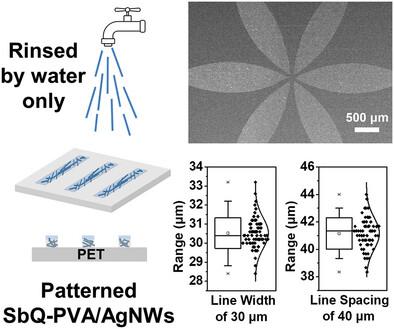
{"title":"Precise Patterning of Flexible Transparent and Conductive Films without Chemical Etchings and Applications in Capacitive Proximity Sensors","authors":"Peiyi Guo, Lijun Ma, Qianru Ge, Jun Shi, Shuxin Li, Shulin Ji","doi":"10.1002/admt.202400476","DOIUrl":null,"url":null,"abstract":"<p>Process microminiaturization is in need not only in chip field, but also in sensor-related industries. Touch panel sensors as an example have their man-machine interactive performance in high relation with the circuit resolution. Traditional etchings by yellow light or laser encounter their resolution limit of ≈50 µm; moreover, former pollution using chemical etchants and latter damage to flexible substrates are inevitable. This paper demonstrates an efficient and green patterning technology for flexible silver nanowire (AgNW) transparent and conductive films, which can enable complicated patterns on various types of substrates with high resolution of a 30 µm line width and 40 µm line spacing. The approach uses a water-soluble photosensitive polymer as the selective protection layer to facilitate the removal of unwanted AgNWs through simple water washing. Due to its good water resistance and mechanical properties, the patterned electrodes exhibit excellent flexibility and environmental stability. As a proof of concept, a capacitive proximity sensor is designed using the patterned AgNW electrodes of the micro feature size, which exhibits excellent proximity sensing performance. The developed patterning technology paves the way to miniaturized feature sizes of different optoelectronic devices for wide applications in fields like new-style displays, man-machine interaction, IoT sensing and intelligent robots.</p>","PeriodicalId":7292,"journal":{"name":"Advanced Materials Technologies","volume":"10 4","pages":""},"PeriodicalIF":6.4000,"publicationDate":"2024-09-04","publicationTypes":"Journal Article","fieldsOfStudy":null,"isOpenAccess":false,"openAccessPdf":"","citationCount":"0","resultStr":null,"platform":"Semanticscholar","paperid":null,"PeriodicalName":"Advanced Materials Technologies","FirstCategoryId":"88","ListUrlMain":"https://advanced.onlinelibrary.wiley.com/doi/10.1002/admt.202400476","RegionNum":3,"RegionCategory":"材料科学","ArticlePicture":[],"TitleCN":null,"AbstractTextCN":null,"PMCID":null,"EPubDate":"","PubModel":"","JCR":"Q1","JCRName":"MATERIALS SCIENCE, MULTIDISCIPLINARY","Score":null,"Total":0}
引用次数: 0
Abstract
Process microminiaturization is in need not only in chip field, but also in sensor-related industries. Touch panel sensors as an example have their man-machine interactive performance in high relation with the circuit resolution. Traditional etchings by yellow light or laser encounter their resolution limit of ≈50 µm; moreover, former pollution using chemical etchants and latter damage to flexible substrates are inevitable. This paper demonstrates an efficient and green patterning technology for flexible silver nanowire (AgNW) transparent and conductive films, which can enable complicated patterns on various types of substrates with high resolution of a 30 µm line width and 40 µm line spacing. The approach uses a water-soluble photosensitive polymer as the selective protection layer to facilitate the removal of unwanted AgNWs through simple water washing. Due to its good water resistance and mechanical properties, the patterned electrodes exhibit excellent flexibility and environmental stability. As a proof of concept, a capacitive proximity sensor is designed using the patterned AgNW electrodes of the micro feature size, which exhibits excellent proximity sensing performance. The developed patterning technology paves the way to miniaturized feature sizes of different optoelectronic devices for wide applications in fields like new-style displays, man-machine interaction, IoT sensing and intelligent robots.
期刊介绍:
Advanced Materials Technologies Advanced Materials Technologies is the new home for all technology-related materials applications research, with particular focus on advanced device design, fabrication and integration, as well as new technologies based on novel materials. It bridges the gap between fundamental laboratory research and industry.


 分享
分享
 求助内容:
求助内容: 应助结果提醒方式:
 扫码关注我们
