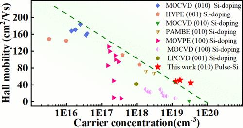
{"title":"High-Efficiency Doping Outcomes in Homoepitaxial β-Ga2O3 Films via Pulsed Si Doping with MOCVD","authors":"Yao Wang, Qian Feng, Wenkai Wu, Yuhong Liu, Yachao Zhang, Jincheng Zhang, Yue Hao","doi":"10.1021/acs.cgd.4c01049","DOIUrl":null,"url":null,"abstract":"Using metal–organic chemical vapor deposition, pulsed Si-doped homoepitaxial gallium oxide (β-Ga<sub>2</sub>O<sub>3</sub>) films were deposited on (010) β-Ga<sub>2</sub>O<sub>3</sub> substrates. The impact of the Si pulse duty cycle on the morphology, structure, and electrical properties of the films was investigated. The full width at half-maximum (fwhm) of the (020) rocking curves for all doped films was less than 55 arcsec, indicating high crystal quality. Employing pulse width modulation of Si doping, as opposed to continuous Si doping, has resulted in a reduction in surface roughness by approximately 2.83 to 9.32 times. Notably, under the conditions of a 0.3 min Si source vent time and a 0.1 min run, an activation ratio of up to 99.1% was achieved, maximizing the electrical performance. This included achieving the lowest resistivity of 0.0042 Ω·cm and an electron mobility of 44.1 cm<sup>2</sup>/(V s) at a carrier concentration of 3.35 × 10<sup>19</sup> cm<sup>–3</sup>. The application of pulsed Si doping provided sufficient diffusion time for Si atoms, enabling effective doping and thereby enhancing the high carrier concentration electrical performance of the films, offering an effective pathway for their use as ohmic contacts in ultrawide-bandgap semiconductor devices.","PeriodicalId":34,"journal":{"name":"Crystal Growth & Design","volume":"37 1","pages":""},"PeriodicalIF":3.4000,"publicationDate":"2024-09-13","publicationTypes":"Journal Article","fieldsOfStudy":null,"isOpenAccess":false,"openAccessPdf":"","citationCount":"0","resultStr":null,"platform":"Semanticscholar","paperid":null,"PeriodicalName":"Crystal Growth & Design","FirstCategoryId":"92","ListUrlMain":"https://doi.org/10.1021/acs.cgd.4c01049","RegionNum":2,"RegionCategory":"化学","ArticlePicture":[],"TitleCN":null,"AbstractTextCN":null,"PMCID":null,"EPubDate":"","PubModel":"","JCR":"Q2","JCRName":"CHEMISTRY, MULTIDISCIPLINARY","Score":null,"Total":0}
引用次数: 0
Abstract
Using metal–organic chemical vapor deposition, pulsed Si-doped homoepitaxial gallium oxide (β-Ga2O3) films were deposited on (010) β-Ga2O3 substrates. The impact of the Si pulse duty cycle on the morphology, structure, and electrical properties of the films was investigated. The full width at half-maximum (fwhm) of the (020) rocking curves for all doped films was less than 55 arcsec, indicating high crystal quality. Employing pulse width modulation of Si doping, as opposed to continuous Si doping, has resulted in a reduction in surface roughness by approximately 2.83 to 9.32 times. Notably, under the conditions of a 0.3 min Si source vent time and a 0.1 min run, an activation ratio of up to 99.1% was achieved, maximizing the electrical performance. This included achieving the lowest resistivity of 0.0042 Ω·cm and an electron mobility of 44.1 cm2/(V s) at a carrier concentration of 3.35 × 1019 cm–3. The application of pulsed Si doping provided sufficient diffusion time for Si atoms, enabling effective doping and thereby enhancing the high carrier concentration electrical performance of the films, offering an effective pathway for their use as ohmic contacts in ultrawide-bandgap semiconductor devices.
期刊介绍:
The aim of Crystal Growth & Design is to stimulate crossfertilization of knowledge among scientists and engineers working in the fields of crystal growth, crystal engineering, and the industrial application of crystalline materials.
Crystal Growth & Design publishes theoretical and experimental studies of the physical, chemical, and biological phenomena and processes related to the design, growth, and application of crystalline materials. Synergistic approaches originating from different disciplines and technologies and integrating the fields of crystal growth, crystal engineering, intermolecular interactions, and industrial application are encouraged.


 分享
分享
 求助内容:
求助内容: 应助结果提醒方式:
 扫码关注我们
