Keisuke Minehisa*, Kaito Nakama, Hidetoshi Hashimoto and Fumitaro Ishikawa*,
{"title":"Homogeneous Large-Scale Synthesis of GaAs/GaInNAs/GaAs Nanowires on a Si Wafer for Devices Operating in the Near-Infrared Region","authors":"Keisuke Minehisa*, Kaito Nakama, Hidetoshi Hashimoto and Fumitaro Ishikawa*, ","doi":"10.1021/acsanm.4c0385510.1021/acsanm.4c03855","DOIUrl":null,"url":null,"abstract":"<p >The synthesis of semiconductor nanowires (NWs) with near-infrared light-absorbing and light-emission properties is presented. Gallium (Ga)-induced vapor–liquid–solid growth is used to produce GaAs/GaInNAs/GaAs core–multishell NWs on a 2 in. Si(111) wafer using plasma-assisted molecular beam epitaxy. The GaInNAs shell consists of 11% indium (In) and varying compositions of nitrogen (N) of up to 1.9%. The NWs serve as an antireflective material, showing that the entire substrate is black. Photoluminescence measurements at room temperature validate the expansion of the operating wavelength into the near-infrared region as the N content in the NWs increases. The GaInNAs sample with 11% In and 1.2% N shows homogeneous luminescence at 1100 nm across the entire 2 in. Si substrate. The reflectance of the NW samples is low, less than 2%, and the absorption edge can be controlled by modifying the composition of In and N indicating the potential application of large-scale photoelectric conversion, such as solar cells.</p>","PeriodicalId":6,"journal":{"name":"ACS Applied Nano Materials","volume":null,"pages":null},"PeriodicalIF":5.3000,"publicationDate":"2024-09-13","publicationTypes":"Journal Article","fieldsOfStudy":null,"isOpenAccess":false,"openAccessPdf":"","citationCount":"0","resultStr":null,"platform":"Semanticscholar","paperid":null,"PeriodicalName":"ACS Applied Nano Materials","FirstCategoryId":"88","ListUrlMain":"https://pubs.acs.org/doi/10.1021/acsanm.4c03855","RegionNum":2,"RegionCategory":"材料科学","ArticlePicture":[],"TitleCN":null,"AbstractTextCN":null,"PMCID":null,"EPubDate":"","PubModel":"","JCR":"Q2","JCRName":"MATERIALS SCIENCE, MULTIDISCIPLINARY","Score":null,"Total":0}
引用次数: 0
Abstract
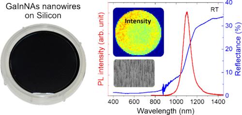
The synthesis of semiconductor nanowires (NWs) with near-infrared light-absorbing and light-emission properties is presented. Gallium (Ga)-induced vapor–liquid–solid growth is used to produce GaAs/GaInNAs/GaAs core–multishell NWs on a 2 in. Si(111) wafer using plasma-assisted molecular beam epitaxy. The GaInNAs shell consists of 11% indium (In) and varying compositions of nitrogen (N) of up to 1.9%. The NWs serve as an antireflective material, showing that the entire substrate is black. Photoluminescence measurements at room temperature validate the expansion of the operating wavelength into the near-infrared region as the N content in the NWs increases. The GaInNAs sample with 11% In and 1.2% N shows homogeneous luminescence at 1100 nm across the entire 2 in. Si substrate. The reflectance of the NW samples is low, less than 2%, and the absorption edge can be controlled by modifying the composition of In and N indicating the potential application of large-scale photoelectric conversion, such as solar cells.
期刊介绍:
ACS Applied Nano Materials is an interdisciplinary journal publishing original research covering all aspects of engineering, chemistry, physics and biology relevant to applications of nanomaterials. The journal is devoted to reports of new and original experimental and theoretical research of an applied nature that integrate knowledge in the areas of materials, engineering, physics, bioscience, and chemistry into important applications of nanomaterials.


 分享
分享
 求助内容:
求助内容: 应助结果提醒方式:
 扫码关注我们
