Elias Semlali*, Evelyne Gil, Geoffrey Avit, Yamina André, Arthur Sauvagnat, Jihen Jridi, Andriy V. Moskalenko, Philip A. Shields, Névine Rochat, Adeline Grenier and Agnès Trassoudaine*,
{"title":"Control of SAG-GaN at the Nanoscale","authors":"Elias Semlali*, Evelyne Gil, Geoffrey Avit, Yamina André, Arthur Sauvagnat, Jihen Jridi, Andriy V. Moskalenko, Philip A. Shields, Névine Rochat, Adeline Grenier and Agnès Trassoudaine*, ","doi":"10.1021/acs.cgd.4c00925","DOIUrl":null,"url":null,"abstract":"<p >Selective area growth (SAG) of GaN nanowires was performed on GaN on c-plane sapphire templates masked with SiN using hydride vapor phase epitaxy (HVPE). GaN nanowires exhibited various morphologies, discussed as a function of the pattern design, the partial pressure of the Ga gaseous precursor, the composition of the carrier gas, and the growth temperature. The morphologies are elucidated by involving a comparative study of growth rates of facets relative to each other. CL measurements showed high emission quality for GaN nanowires grown at 930 °C. This work places HVPE as an effective epitaxial technique for growing III–N nanostructure-based devices at a low cost.</p>","PeriodicalId":34,"journal":{"name":"Crystal Growth & Design","volume":"24 21","pages":"8907–8913 8907–8913"},"PeriodicalIF":3.4000,"publicationDate":"2024-10-09","publicationTypes":"Journal Article","fieldsOfStudy":null,"isOpenAccess":false,"openAccessPdf":"","citationCount":"0","resultStr":null,"platform":"Semanticscholar","paperid":null,"PeriodicalName":"Crystal Growth & Design","FirstCategoryId":"92","ListUrlMain":"https://pubs.acs.org/doi/10.1021/acs.cgd.4c00925","RegionNum":2,"RegionCategory":"化学","ArticlePicture":[],"TitleCN":null,"AbstractTextCN":null,"PMCID":null,"EPubDate":"","PubModel":"","JCR":"Q2","JCRName":"CHEMISTRY, MULTIDISCIPLINARY","Score":null,"Total":0}
引用次数: 0
Abstract
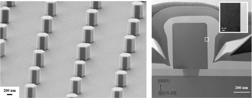
Selective area growth (SAG) of GaN nanowires was performed on GaN on c-plane sapphire templates masked with SiN using hydride vapor phase epitaxy (HVPE). GaN nanowires exhibited various morphologies, discussed as a function of the pattern design, the partial pressure of the Ga gaseous precursor, the composition of the carrier gas, and the growth temperature. The morphologies are elucidated by involving a comparative study of growth rates of facets relative to each other. CL measurements showed high emission quality for GaN nanowires grown at 930 °C. This work places HVPE as an effective epitaxial technique for growing III–N nanostructure-based devices at a low cost.
期刊介绍:
The aim of Crystal Growth & Design is to stimulate crossfertilization of knowledge among scientists and engineers working in the fields of crystal growth, crystal engineering, and the industrial application of crystalline materials.
Crystal Growth & Design publishes theoretical and experimental studies of the physical, chemical, and biological phenomena and processes related to the design, growth, and application of crystalline materials. Synergistic approaches originating from different disciplines and technologies and integrating the fields of crystal growth, crystal engineering, intermolecular interactions, and industrial application are encouraged.


 分享
分享
 求助内容:
求助内容: 应助结果提醒方式:
 扫码关注我们
