Shinichiro Hatta*, Shimpei Higaki, Hiroshi Okuyama and Tetsuya Aruga*,
{"title":"Twin-Free Growth of Ultrathin Bi2Te3 Films on CaF2(111)/Si(111)","authors":"Shinichiro Hatta*, Shimpei Higaki, Hiroshi Okuyama and Tetsuya Aruga*, ","doi":"10.1021/acs.cgd.4c01258","DOIUrl":null,"url":null,"abstract":"<p >The CaF<sub>2</sub>(111) surface has no dangling bond, which allows it to be used as a substrate for the van der Waals epitaxy of layered materials. In addition, a CaF<sub>2</sub>(111) thin film can serve as a crystalline insulating buffer on Si(111) due to good lattice matching. We investigated the heteroepitaxy of topological insulator Bi<sub>2</sub>Te<sub>3</sub> on a CaF<sub>2</sub>(111) thin film by low-energy electron diffraction (LEED), angle-resolved photoelectron spectroscopy, and conductivity measurements. Well-ordered Bi<sub>2</sub>Te<sub>3</sub>(111) films were obtained by molecular beam epitaxy on the substrate at 370 K. As the thickness increased above one quintuple layer (QL), the lateral domain size rapidly increased, and one domain became dominant. The twin-free structure of the 5 QL film was confirmed by the dynamical LEED calculation. The films with thickness above 2 QL exhibited metallic conduction through the surface band and the bulk-like conduction band. The observed rapid increase in conductivity at 4–5 QL is attributed to the thickness limit of the topological surface state.</p>","PeriodicalId":34,"journal":{"name":"Crystal Growth & Design","volume":"24 23","pages":"10038–10045 10038–10045"},"PeriodicalIF":3.4000,"publicationDate":"2024-11-14","publicationTypes":"Journal Article","fieldsOfStudy":null,"isOpenAccess":false,"openAccessPdf":"","citationCount":"0","resultStr":null,"platform":"Semanticscholar","paperid":null,"PeriodicalName":"Crystal Growth & Design","FirstCategoryId":"92","ListUrlMain":"https://pubs.acs.org/doi/10.1021/acs.cgd.4c01258","RegionNum":2,"RegionCategory":"化学","ArticlePicture":[],"TitleCN":null,"AbstractTextCN":null,"PMCID":null,"EPubDate":"","PubModel":"","JCR":"Q2","JCRName":"CHEMISTRY, MULTIDISCIPLINARY","Score":null,"Total":0}
引用次数: 0
Abstract
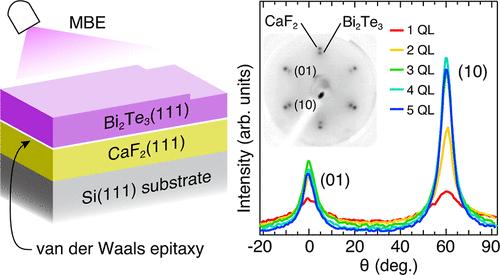
The CaF2(111) surface has no dangling bond, which allows it to be used as a substrate for the van der Waals epitaxy of layered materials. In addition, a CaF2(111) thin film can serve as a crystalline insulating buffer on Si(111) due to good lattice matching. We investigated the heteroepitaxy of topological insulator Bi2Te3 on a CaF2(111) thin film by low-energy electron diffraction (LEED), angle-resolved photoelectron spectroscopy, and conductivity measurements. Well-ordered Bi2Te3(111) films were obtained by molecular beam epitaxy on the substrate at 370 K. As the thickness increased above one quintuple layer (QL), the lateral domain size rapidly increased, and one domain became dominant. The twin-free structure of the 5 QL film was confirmed by the dynamical LEED calculation. The films with thickness above 2 QL exhibited metallic conduction through the surface band and the bulk-like conduction band. The observed rapid increase in conductivity at 4–5 QL is attributed to the thickness limit of the topological surface state.
期刊介绍:
The aim of Crystal Growth & Design is to stimulate crossfertilization of knowledge among scientists and engineers working in the fields of crystal growth, crystal engineering, and the industrial application of crystalline materials.
Crystal Growth & Design publishes theoretical and experimental studies of the physical, chemical, and biological phenomena and processes related to the design, growth, and application of crystalline materials. Synergistic approaches originating from different disciplines and technologies and integrating the fields of crystal growth, crystal engineering, intermolecular interactions, and industrial application are encouraged.


 分享
分享
 求助内容:
求助内容: 应助结果提醒方式:
 扫码关注我们
