Asad A. Thahe, Ali Dahi, Motahher A. Qaeed, Omar F. Farhat, Hazri Bakhtiar and Nageh K. Allam
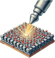
{"title":"Engineered etching and laser treatment of porous silicon for enhanced sensitivity and speed of Pt/n-PSi/Pt UV photodetectors","authors":"Asad A. Thahe, Ali Dahi, Motahher A. Qaeed, Omar F. Farhat, Hazri Bakhtiar and Nageh K. Allam","doi":"10.1039/D5NA00137D","DOIUrl":null,"url":null,"abstract":"<p >Silicon-based photodetectors offer notable advantages in cost, performance, and reliability. However, while nanoscale silicon (porous silicon, PSi) effectively emits visible light, it remains inefficient as an indirect-bandgap semiconductor. To improve its optoelectronic properties, coupling silicon with a wide-bandgap semiconductor is a promising strategy. In this study, nanoporous silicon (n-PSi) films were fabricated from an n-type Si (111) wafer using optimized photoelectrochemical etching (PECE). These films were then irradiated with Q-switched Nd:YAG laser pulses (3, 5, 10, and 20 pulses) at a fixed wavelength of 1068 nm, with pulse durations ranging from 3 to 20 ns and a constant repetition rate of 10 Hz. The structural, morphological, and optical properties of both as-prepared and laser-annealed n-PSi samples were characterized using various analytical techniques. Among the laser-treated samples, n-PSi subjected to three laser pulses exhibited the highest crystallinity and largest crystallite size (∼87.02 nm). This optimized sample was selected for fabricating a Pt/n-PSi/Pt metal–semiconductor–metal (MSM) ultraviolet (UV) photodetector. The photoluminescence spectra of the fabricated devices revealed strong near-band-edge (NBE) emission, with a violet band centered around 523 nm, corresponding to a bandgap energy of 2.36 eV. The <em>I</em>–<em>V</em> characteristics of the MSM UV photodetectors were analyzed under dark conditions and 380 nm UV illumination. The device demonstrated high photosensitivity (951.28), excellent responsivity (2.01 A W<small><sup>−1</sup></small>), and fast response (0.44 s) and recovery (0.48 s) times, outperforming conventional photodetectors. This approach provides a viable pathway for tuning nanomaterials with tailored properties for high-performance nanodevices. The fabricated MSM UV photodetectors show great potential for next-generation optoelectronic applications.</p>","PeriodicalId":18806,"journal":{"name":"Nanoscale Advances","volume":" 10","pages":" 2955-2966"},"PeriodicalIF":4.6000,"publicationDate":"2025-03-27","publicationTypes":"Journal Article","fieldsOfStudy":null,"isOpenAccess":false,"openAccessPdf":"https://www.ncbi.nlm.nih.gov/pmc/articles/PMC11960784/pdf/","citationCount":"0","resultStr":null,"platform":"Semanticscholar","paperid":null,"PeriodicalName":"Nanoscale Advances","FirstCategoryId":"88","ListUrlMain":"https://pubs.rsc.org/en/content/articlelanding/2025/na/d5na00137d","RegionNum":3,"RegionCategory":"材料科学","ArticlePicture":[],"TitleCN":null,"AbstractTextCN":null,"PMCID":null,"EPubDate":"","PubModel":"","JCR":"Q2","JCRName":"CHEMISTRY, MULTIDISCIPLINARY","Score":null,"Total":0}
引用次数: 0
Abstract
Silicon-based photodetectors offer notable advantages in cost, performance, and reliability. However, while nanoscale silicon (porous silicon, PSi) effectively emits visible light, it remains inefficient as an indirect-bandgap semiconductor. To improve its optoelectronic properties, coupling silicon with a wide-bandgap semiconductor is a promising strategy. In this study, nanoporous silicon (n-PSi) films were fabricated from an n-type Si (111) wafer using optimized photoelectrochemical etching (PECE). These films were then irradiated with Q-switched Nd:YAG laser pulses (3, 5, 10, and 20 pulses) at a fixed wavelength of 1068 nm, with pulse durations ranging from 3 to 20 ns and a constant repetition rate of 10 Hz. The structural, morphological, and optical properties of both as-prepared and laser-annealed n-PSi samples were characterized using various analytical techniques. Among the laser-treated samples, n-PSi subjected to three laser pulses exhibited the highest crystallinity and largest crystallite size (∼87.02 nm). This optimized sample was selected for fabricating a Pt/n-PSi/Pt metal–semiconductor–metal (MSM) ultraviolet (UV) photodetector. The photoluminescence spectra of the fabricated devices revealed strong near-band-edge (NBE) emission, with a violet band centered around 523 nm, corresponding to a bandgap energy of 2.36 eV. The I–V characteristics of the MSM UV photodetectors were analyzed under dark conditions and 380 nm UV illumination. The device demonstrated high photosensitivity (951.28), excellent responsivity (2.01 A W−1), and fast response (0.44 s) and recovery (0.48 s) times, outperforming conventional photodetectors. This approach provides a viable pathway for tuning nanomaterials with tailored properties for high-performance nanodevices. The fabricated MSM UV photodetectors show great potential for next-generation optoelectronic applications.


 分享
分享
 求助内容:
求助内容: 应助结果提醒方式:
 扫码关注我们
