{"title":"封装微电子封装中环氧模塑料 (EMC) 与金属之间分层的实验和数值研究","authors":"M.-K. Shih, Y.-H. Liu, G.-S. Lin, E. Hsu, J. Yang","doi":"10.1007/s40799-023-00679-5","DOIUrl":null,"url":null,"abstract":"<div><p>Microelectronics packages play a vital role in not only interconnecting the electronic signals from the die to the printed circuit board (PCB), but also in protecting the chips during the manufacturing process and their subsequent service lives. Epoxy molding compound (EMC) is widely used in electronic packaging due to its superior processing capability and low circuit signal delay. However, interfacial delamination is a common problem in encapsulated silicon devices, particularly at the interface between the copper leadframe (LF) pads and the EMC due to the weaker adhesion strength. Accordingly, the present study employs a double cantilever beam (DCB) experimental testing method and a numerical model based on the virtual crack closure technique (VCCT) to investigate the fracture behavior at the EMC/Cu LF interface in a quad flat no leads (QFN) package. The experiments are performed on an MTS-Acumen microforce tester equipped with a load unit capable of applying a force of 0.01 to 1250 N with a displacement resolution of 0.1 μm. The DCB specimens are prepared with a pre-crack length of 12 mm. The validity of the simulation model is confirmed by comparing the predicted values of the critical strain energy release rate (SERR, G<sub>c</sub>) between the EMC and the copper LF pads with the experimental observations. In general, the results show that the G<sub>c</sub> value provides a useful parameter for evaluating the delamination risk of encapsulated microelectronics packages and assessing the reliability of alternative package architectures.</p></div>","PeriodicalId":553,"journal":{"name":"Experimental Techniques","volume":"48 4","pages":"599 - 609"},"PeriodicalIF":1.8000,"publicationDate":"2023-10-27","publicationTypes":"Journal Article","fieldsOfStudy":null,"isOpenAccess":false,"openAccessPdf":"","citationCount":"0","resultStr":"{\"title\":\"Experimental and Numerical Investigation of Delamination Between Epoxy Molding Compound (EMC) and Metal in Encapsulated Microelectronic Packages\",\"authors\":\"M.-K. Shih, Y.-H. Liu, G.-S. Lin, E. Hsu, J. Yang\",\"doi\":\"10.1007/s40799-023-00679-5\",\"DOIUrl\":null,\"url\":null,\"abstract\":\"<div><p>Microelectronics packages play a vital role in not only interconnecting the electronic signals from the die to the printed circuit board (PCB), but also in protecting the chips during the manufacturing process and their subsequent service lives. Epoxy molding compound (EMC) is widely used in electronic packaging due to its superior processing capability and low circuit signal delay. However, interfacial delamination is a common problem in encapsulated silicon devices, particularly at the interface between the copper leadframe (LF) pads and the EMC due to the weaker adhesion strength. Accordingly, the present study employs a double cantilever beam (DCB) experimental testing method and a numerical model based on the virtual crack closure technique (VCCT) to investigate the fracture behavior at the EMC/Cu LF interface in a quad flat no leads (QFN) package. The experiments are performed on an MTS-Acumen microforce tester equipped with a load unit capable of applying a force of 0.01 to 1250 N with a displacement resolution of 0.1 μm. The DCB specimens are prepared with a pre-crack length of 12 mm. The validity of the simulation model is confirmed by comparing the predicted values of the critical strain energy release rate (SERR, G<sub>c</sub>) between the EMC and the copper LF pads with the experimental observations. In general, the results show that the G<sub>c</sub> value provides a useful parameter for evaluating the delamination risk of encapsulated microelectronics packages and assessing the reliability of alternative package architectures.</p></div>\",\"PeriodicalId\":553,\"journal\":{\"name\":\"Experimental Techniques\",\"volume\":\"48 4\",\"pages\":\"599 - 609\"},\"PeriodicalIF\":1.8000,\"publicationDate\":\"2023-10-27\",\"publicationTypes\":\"Journal Article\",\"fieldsOfStudy\":null,\"isOpenAccess\":false,\"openAccessPdf\":\"\",\"citationCount\":\"0\",\"resultStr\":null,\"platform\":\"Semanticscholar\",\"paperid\":null,\"PeriodicalName\":\"Experimental Techniques\",\"FirstCategoryId\":\"5\",\"ListUrlMain\":\"https://link.springer.com/article/10.1007/s40799-023-00679-5\",\"RegionNum\":4,\"RegionCategory\":\"工程技术\",\"ArticlePicture\":[],\"TitleCN\":null,\"AbstractTextCN\":null,\"PMCID\":null,\"EPubDate\":\"\",\"PubModel\":\"\",\"JCR\":\"Q3\",\"JCRName\":\"ENGINEERING, MECHANICAL\",\"Score\":null,\"Total\":0}","platform":"Semanticscholar","paperid":null,"PeriodicalName":"Experimental Techniques","FirstCategoryId":"5","ListUrlMain":"https://link.springer.com/article/10.1007/s40799-023-00679-5","RegionNum":4,"RegionCategory":"工程技术","ArticlePicture":[],"TitleCN":null,"AbstractTextCN":null,"PMCID":null,"EPubDate":"","PubModel":"","JCR":"Q3","JCRName":"ENGINEERING, MECHANICAL","Score":null,"Total":0}
Experimental and Numerical Investigation of Delamination Between Epoxy Molding Compound (EMC) and Metal in Encapsulated Microelectronic Packages
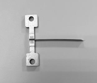
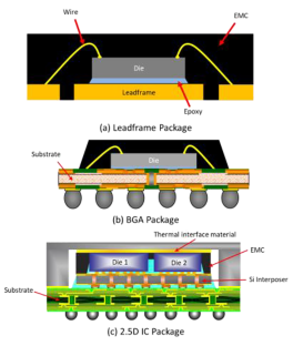
Microelectronics packages play a vital role in not only interconnecting the electronic signals from the die to the printed circuit board (PCB), but also in protecting the chips during the manufacturing process and their subsequent service lives. Epoxy molding compound (EMC) is widely used in electronic packaging due to its superior processing capability and low circuit signal delay. However, interfacial delamination is a common problem in encapsulated silicon devices, particularly at the interface between the copper leadframe (LF) pads and the EMC due to the weaker adhesion strength. Accordingly, the present study employs a double cantilever beam (DCB) experimental testing method and a numerical model based on the virtual crack closure technique (VCCT) to investigate the fracture behavior at the EMC/Cu LF interface in a quad flat no leads (QFN) package. The experiments are performed on an MTS-Acumen microforce tester equipped with a load unit capable of applying a force of 0.01 to 1250 N with a displacement resolution of 0.1 μm. The DCB specimens are prepared with a pre-crack length of 12 mm. The validity of the simulation model is confirmed by comparing the predicted values of the critical strain energy release rate (SERR, Gc) between the EMC and the copper LF pads with the experimental observations. In general, the results show that the Gc value provides a useful parameter for evaluating the delamination risk of encapsulated microelectronics packages and assessing the reliability of alternative package architectures.
期刊介绍:
Experimental Techniques is a bimonthly interdisciplinary publication of the Society for Experimental Mechanics focusing on the development, application and tutorial of experimental mechanics techniques.
The purpose for Experimental Techniques is to promote pedagogical, technical and practical advancements in experimental mechanics while supporting the Society''s mission and commitment to interdisciplinary application, research and development, education, and active promotion of experimental methods to:
- Increase the knowledge of physical phenomena
- Further the understanding of the behavior of materials, structures, and systems
- Provide the necessary physical observations necessary to improve and assess new analytical and computational approaches.


 分享
分享
 求助内容:
求助内容: 应助结果提醒方式:
 扫码关注我们
