Nicholas Hunwick, Xiaolei Liu, Mustafa Togay, John M. Walls, Jake Bowers and Patrick J. M. Isherwood
{"title":"氧对碲化镉太阳能电池中作为背缓冲层的氧化镍的影响","authors":"Nicholas Hunwick, Xiaolei Liu, Mustafa Togay, John M. Walls, Jake Bowers and Patrick J. M. Isherwood","doi":"10.1039/D4YA00125G","DOIUrl":null,"url":null,"abstract":"<p >Thin film CdTe-based photovoltaic devices have achieved high efficiency above 22%. However, the device performance is limited by large open circuit voltage deficit. One of the primary reasons is non-ohmic back contacts. In this work, nickel oxide is used as a back buffer layer to form an ohmic back contact. We comprehensively investigate oxygen effects during sputtering on film properties and device performance. Increased oxygen in the deposition environment led to darker films, increased carrier concentration, decreased mobility and decreased resistivity. X-ray photoelectron spectroscopy showed peak shifts favouring Ni<small><sup>3+</sup></small> over Ni<small><sup>2+</sup></small>, and X-ray diffraction demonstrated that crystallinity hit a peak at around 5% oxygen input. The NiO back buffer layer improves device performance by reducing barrier height at the gold back contact and improving valence band offset at the CdTe/NiO interface. The NiO layer deposited without oxygen improved the <em>V</em><small><sub>oc</sub></small> to 710 mV, from a baseline of 585 mV. At 5% and 20% oxygen content during deposition, efficiency improved relative to the reference due to an increase in open circuit voltage (<em>V</em><small><sub>oc</sub></small>) and short circuit current (<em>J</em><small><sub>sc</sub></small>). <em>V</em><small><sub>oc</sub></small> increase is due to improved valence band offset between CdTe and NiO. The large conduction band offset also reflects minority carriers away from the CdTe/NiO interface and reduces interface recombination. SCAPS simulations demonstrated that an increase in valence band offset has shown pronounced effects of both s-kinks and rollover.</p>","PeriodicalId":72913,"journal":{"name":"Energy advances","volume":" 7","pages":" 1746-1753"},"PeriodicalIF":4.3000,"publicationDate":"2024-05-30","publicationTypes":"Journal Article","fieldsOfStudy":null,"isOpenAccess":false,"openAccessPdf":"https://pubs.rsc.org/en/content/articlepdf/2024/ya/d4ya00125g?page=search","citationCount":"0","resultStr":"{\"title\":\"The effect of oxygen on NiO as a back buffer layer in CdTe solar cells\",\"authors\":\"Nicholas Hunwick, Xiaolei Liu, Mustafa Togay, John M. Walls, Jake Bowers and Patrick J. M. Isherwood\",\"doi\":\"10.1039/D4YA00125G\",\"DOIUrl\":null,\"url\":null,\"abstract\":\"<p >Thin film CdTe-based photovoltaic devices have achieved high efficiency above 22%. However, the device performance is limited by large open circuit voltage deficit. One of the primary reasons is non-ohmic back contacts. In this work, nickel oxide is used as a back buffer layer to form an ohmic back contact. We comprehensively investigate oxygen effects during sputtering on film properties and device performance. Increased oxygen in the deposition environment led to darker films, increased carrier concentration, decreased mobility and decreased resistivity. X-ray photoelectron spectroscopy showed peak shifts favouring Ni<small><sup>3+</sup></small> over Ni<small><sup>2+</sup></small>, and X-ray diffraction demonstrated that crystallinity hit a peak at around 5% oxygen input. The NiO back buffer layer improves device performance by reducing barrier height at the gold back contact and improving valence band offset at the CdTe/NiO interface. The NiO layer deposited without oxygen improved the <em>V</em><small><sub>oc</sub></small> to 710 mV, from a baseline of 585 mV. At 5% and 20% oxygen content during deposition, efficiency improved relative to the reference due to an increase in open circuit voltage (<em>V</em><small><sub>oc</sub></small>) and short circuit current (<em>J</em><small><sub>sc</sub></small>). <em>V</em><small><sub>oc</sub></small> increase is due to improved valence band offset between CdTe and NiO. The large conduction band offset also reflects minority carriers away from the CdTe/NiO interface and reduces interface recombination. SCAPS simulations demonstrated that an increase in valence band offset has shown pronounced effects of both s-kinks and rollover.</p>\",\"PeriodicalId\":72913,\"journal\":{\"name\":\"Energy advances\",\"volume\":\" 7\",\"pages\":\" 1746-1753\"},\"PeriodicalIF\":4.3000,\"publicationDate\":\"2024-05-30\",\"publicationTypes\":\"Journal Article\",\"fieldsOfStudy\":null,\"isOpenAccess\":false,\"openAccessPdf\":\"https://pubs.rsc.org/en/content/articlepdf/2024/ya/d4ya00125g?page=search\",\"citationCount\":\"0\",\"resultStr\":null,\"platform\":\"Semanticscholar\",\"paperid\":null,\"PeriodicalName\":\"Energy advances\",\"FirstCategoryId\":\"1085\",\"ListUrlMain\":\"https://pubs.rsc.org/en/content/articlelanding/2024/ya/d4ya00125g\",\"RegionNum\":0,\"RegionCategory\":null,\"ArticlePicture\":[],\"TitleCN\":null,\"AbstractTextCN\":null,\"PMCID\":null,\"EPubDate\":\"\",\"PubModel\":\"\",\"JCR\":\"Q2\",\"JCRName\":\"CHEMISTRY, PHYSICAL\",\"Score\":null,\"Total\":0}","platform":"Semanticscholar","paperid":null,"PeriodicalName":"Energy advances","FirstCategoryId":"1085","ListUrlMain":"https://pubs.rsc.org/en/content/articlelanding/2024/ya/d4ya00125g","RegionNum":0,"RegionCategory":null,"ArticlePicture":[],"TitleCN":null,"AbstractTextCN":null,"PMCID":null,"EPubDate":"","PubModel":"","JCR":"Q2","JCRName":"CHEMISTRY, PHYSICAL","Score":null,"Total":0}
引用次数: 0
摘要
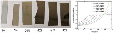
基于碲化镉的薄膜光伏器件已经实现了 22% 以上的高效率。然而,该器件的性能受到开路电压缺口较大的限制。其中一个主要原因是非欧姆背触点。在这项研究中,氧化镍被用作背面缓冲层,以形成欧姆背接触。我们全面研究了溅射过程中氧对薄膜特性和器件性能的影响。沉积环境中氧的增加导致薄膜颜色变深、载流子浓度增加、迁移率降低和电阻率下降。X 射线光电子能谱显示,Ni3+ 的峰值偏向于 Ni2+,而 X 射线衍射则表明,在氧气输入量为 5%左右时,结晶度达到峰值。氧化镍背缓冲层可降低金背接触处的势垒高度,改善碲化镉/氧化镍界面的价带偏移,从而提高器件性能。无氧沉积的氧化镍层将 Voc 从 585mV 的基线提高到 710mV。在沉积过程中,氧含量分别为 5%和 20%时,由于开路电压(Voc)和短路电流(Jsc)的增加,效率相对于参考值有所提高。Voc 的增加是由于碲化镉和氧化镍之间价带偏移的改善。较大的导带偏移也将少数载流子从碲化镉/氧化镍界面反射出去,减少了界面重组。SCAPS 模拟表明,价带偏移的增加对 S 形扭结和翻转都有明显的影响。
The effect of oxygen on NiO as a back buffer layer in CdTe solar cells
Thin film CdTe-based photovoltaic devices have achieved high efficiency above 22%. However, the device performance is limited by large open circuit voltage deficit. One of the primary reasons is non-ohmic back contacts. In this work, nickel oxide is used as a back buffer layer to form an ohmic back contact. We comprehensively investigate oxygen effects during sputtering on film properties and device performance. Increased oxygen in the deposition environment led to darker films, increased carrier concentration, decreased mobility and decreased resistivity. X-ray photoelectron spectroscopy showed peak shifts favouring Ni3+ over Ni2+, and X-ray diffraction demonstrated that crystallinity hit a peak at around 5% oxygen input. The NiO back buffer layer improves device performance by reducing barrier height at the gold back contact and improving valence band offset at the CdTe/NiO interface. The NiO layer deposited without oxygen improved the Voc to 710 mV, from a baseline of 585 mV. At 5% and 20% oxygen content during deposition, efficiency improved relative to the reference due to an increase in open circuit voltage (Voc) and short circuit current (Jsc). Voc increase is due to improved valence band offset between CdTe and NiO. The large conduction band offset also reflects minority carriers away from the CdTe/NiO interface and reduces interface recombination. SCAPS simulations demonstrated that an increase in valence band offset has shown pronounced effects of both s-kinks and rollover.


 分享
分享

 求助内容:
求助内容: 应助结果提醒方式:
 扫码关注我们
