Udari Wijesinghe, William D. Tetlow, Pietro Maiello, Nicole Fleck, Graeme O’Dowd, Neil S. Beattie, Giulia Longo* and Oliver S. Hutter*,
{"title":"通过光子固化实现光电子学用结晶硒化锑薄膜","authors":"Udari Wijesinghe, William D. Tetlow, Pietro Maiello, Nicole Fleck, Graeme O’Dowd, Neil S. Beattie, Giulia Longo* and Oliver S. Hutter*, ","doi":"10.1021/acs.chemmater.4c00540","DOIUrl":null,"url":null,"abstract":"<p >Thermal annealing is the most common postdeposition technique used to crystallize antimony selenide (Sb<sub>2</sub>Se<sub>3</sub>) thin films. However, due to slow processing speeds and a high energy cost, it is incompatible with the upscaling and commercialization of Sb<sub>2</sub>Se<sub>3</sub> for future photovoltaics. Herein, for the first time, a fast-annealing technique that uses millisecond light pulses to deliver energy to the sample is adapted to cure thermally evaporated Sb<sub>2</sub>Se<sub>3</sub> films. This study demonstrates how photonic curing (PC) conditions affect the outcome of Sb<sub>2</sub>Se<sub>3</sub> phase conversion from amorphous to crystalline by evaluating the films’ crystalline, morphological, and optical properties. We show that Sb<sub>2</sub>Se<sub>3</sub> is readily converted under a variety of different conditions, but the zone where suitable films for optoelectronic applications are obtained is a small region of the parameter space. Sb<sub>2</sub>Se<sub>3</sub> annealing with short pulses (<3 ms) shows significant damage to the sample, while using longer pulses (>5 ms) and a 4–5 J cm<sup>–2</sup> radiant energy produces (211)- and (221)-oriented crystalline Sb<sub>2</sub>Se<sub>3</sub> with minimal to no damage to the sample. A proof-of-concept photonically cured Sb<sub>2</sub>Se<sub>3</sub> photovoltaic device is demonstrated. PC is a promising annealing method for large-area, high-throughput annealing of Sb<sub>2</sub>Se<sub>3</sub> with various potential applications in Sb<sub>2</sub>Se<sub>3</sub> photovoltaics.</p>","PeriodicalId":33,"journal":{"name":"Chemistry of Materials","volume":"36 12","pages":"6027–6037"},"PeriodicalIF":7.0000,"publicationDate":"2024-06-06","publicationTypes":"Journal Article","fieldsOfStudy":null,"isOpenAccess":false,"openAccessPdf":"https://pubs.acs.org/doi/epdf/10.1021/acs.chemmater.4c00540","citationCount":"0","resultStr":"{\"title\":\"Crystalline Antimony Selenide Thin Films for Optoelectronics through Photonic Curing\",\"authors\":\"Udari Wijesinghe, William D. Tetlow, Pietro Maiello, Nicole Fleck, Graeme O’Dowd, Neil S. Beattie, Giulia Longo* and Oliver S. Hutter*, \",\"doi\":\"10.1021/acs.chemmater.4c00540\",\"DOIUrl\":null,\"url\":null,\"abstract\":\"<p >Thermal annealing is the most common postdeposition technique used to crystallize antimony selenide (Sb<sub>2</sub>Se<sub>3</sub>) thin films. However, due to slow processing speeds and a high energy cost, it is incompatible with the upscaling and commercialization of Sb<sub>2</sub>Se<sub>3</sub> for future photovoltaics. Herein, for the first time, a fast-annealing technique that uses millisecond light pulses to deliver energy to the sample is adapted to cure thermally evaporated Sb<sub>2</sub>Se<sub>3</sub> films. This study demonstrates how photonic curing (PC) conditions affect the outcome of Sb<sub>2</sub>Se<sub>3</sub> phase conversion from amorphous to crystalline by evaluating the films’ crystalline, morphological, and optical properties. We show that Sb<sub>2</sub>Se<sub>3</sub> is readily converted under a variety of different conditions, but the zone where suitable films for optoelectronic applications are obtained is a small region of the parameter space. Sb<sub>2</sub>Se<sub>3</sub> annealing with short pulses (<3 ms) shows significant damage to the sample, while using longer pulses (>5 ms) and a 4–5 J cm<sup>–2</sup> radiant energy produces (211)- and (221)-oriented crystalline Sb<sub>2</sub>Se<sub>3</sub> with minimal to no damage to the sample. A proof-of-concept photonically cured Sb<sub>2</sub>Se<sub>3</sub> photovoltaic device is demonstrated. PC is a promising annealing method for large-area, high-throughput annealing of Sb<sub>2</sub>Se<sub>3</sub> with various potential applications in Sb<sub>2</sub>Se<sub>3</sub> photovoltaics.</p>\",\"PeriodicalId\":33,\"journal\":{\"name\":\"Chemistry of Materials\",\"volume\":\"36 12\",\"pages\":\"6027–6037\"},\"PeriodicalIF\":7.0000,\"publicationDate\":\"2024-06-06\",\"publicationTypes\":\"Journal Article\",\"fieldsOfStudy\":null,\"isOpenAccess\":false,\"openAccessPdf\":\"https://pubs.acs.org/doi/epdf/10.1021/acs.chemmater.4c00540\",\"citationCount\":\"0\",\"resultStr\":null,\"platform\":\"Semanticscholar\",\"paperid\":null,\"PeriodicalName\":\"Chemistry of Materials\",\"FirstCategoryId\":\"88\",\"ListUrlMain\":\"https://pubs.acs.org/doi/10.1021/acs.chemmater.4c00540\",\"RegionNum\":2,\"RegionCategory\":\"材料科学\",\"ArticlePicture\":[],\"TitleCN\":null,\"AbstractTextCN\":null,\"PMCID\":null,\"EPubDate\":\"\",\"PubModel\":\"\",\"JCR\":\"Q2\",\"JCRName\":\"CHEMISTRY, PHYSICAL\",\"Score\":null,\"Total\":0}","platform":"Semanticscholar","paperid":null,"PeriodicalName":"Chemistry of Materials","FirstCategoryId":"88","ListUrlMain":"https://pubs.acs.org/doi/10.1021/acs.chemmater.4c00540","RegionNum":2,"RegionCategory":"材料科学","ArticlePicture":[],"TitleCN":null,"AbstractTextCN":null,"PMCID":null,"EPubDate":"","PubModel":"","JCR":"Q2","JCRName":"CHEMISTRY, PHYSICAL","Score":null,"Total":0}
Crystalline Antimony Selenide Thin Films for Optoelectronics through Photonic Curing
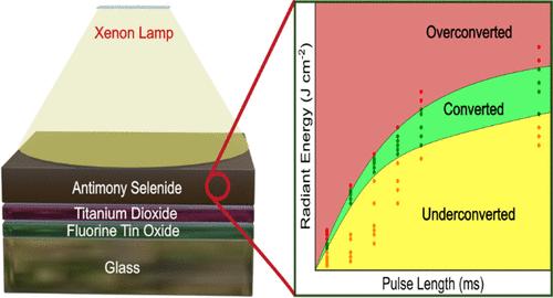
Thermal annealing is the most common postdeposition technique used to crystallize antimony selenide (Sb2Se3) thin films. However, due to slow processing speeds and a high energy cost, it is incompatible with the upscaling and commercialization of Sb2Se3 for future photovoltaics. Herein, for the first time, a fast-annealing technique that uses millisecond light pulses to deliver energy to the sample is adapted to cure thermally evaporated Sb2Se3 films. This study demonstrates how photonic curing (PC) conditions affect the outcome of Sb2Se3 phase conversion from amorphous to crystalline by evaluating the films’ crystalline, morphological, and optical properties. We show that Sb2Se3 is readily converted under a variety of different conditions, but the zone where suitable films for optoelectronic applications are obtained is a small region of the parameter space. Sb2Se3 annealing with short pulses (<3 ms) shows significant damage to the sample, while using longer pulses (>5 ms) and a 4–5 J cm–2 radiant energy produces (211)- and (221)-oriented crystalline Sb2Se3 with minimal to no damage to the sample. A proof-of-concept photonically cured Sb2Se3 photovoltaic device is demonstrated. PC is a promising annealing method for large-area, high-throughput annealing of Sb2Se3 with various potential applications in Sb2Se3 photovoltaics.
期刊介绍:
The journal Chemistry of Materials focuses on publishing original research at the intersection of materials science and chemistry. The studies published in the journal involve chemistry as a prominent component and explore topics such as the design, synthesis, characterization, processing, understanding, and application of functional or potentially functional materials. The journal covers various areas of interest, including inorganic and organic solid-state chemistry, nanomaterials, biomaterials, thin films and polymers, and composite/hybrid materials. The journal particularly seeks papers that highlight the creation or development of innovative materials with novel optical, electrical, magnetic, catalytic, or mechanical properties. It is essential that manuscripts on these topics have a primary focus on the chemistry of materials and represent a significant advancement compared to prior research. Before external reviews are sought, submitted manuscripts undergo a review process by a minimum of two editors to ensure their appropriateness for the journal and the presence of sufficient evidence of a significant advance that will be of broad interest to the materials chemistry community.


 分享
分享
 求助内容:
求助内容: 应助结果提醒方式:
 扫码关注我们
