Moritz Quincke, Manuel Mundszinger, Johannes Biskupek, Ute Kaiser
{"title":"三层 MoS2 叠层中间层的缺陷密度和原子缺陷识别。","authors":"Moritz Quincke, Manuel Mundszinger, Johannes Biskupek, Ute Kaiser","doi":"10.1021/acs.nanolett.4c02391","DOIUrl":null,"url":null,"abstract":"<p><p>Molybdenum disulfide (MoS<sub>2</sub>) is one of the most intriguing two-dimensional materials, and moreover, its single atomic defects can significantly alter the properties. These defects can be both imaged and engineered using spherical and chromatic aberration-corrected high-resolution transmission electron microscopy (C<sub>C</sub>/C<sub>S</sub>-corrected HRTEM). In a few-layer stack, several atoms are vertically aligned in one atomic column. Therefore, it is challenging to determine the positions of missing atoms and the damage cross-section, particularly in the not directly accessible middle layers. In this study, we introduce a technique for extracting subtle intensity differences in C<sub>C</sub>/C<sub>S</sub>-corrected HRTEM images. By exploiting the crystal structure of the material, our method discerns chalcogen vacancies even in the middle layer of trilayer MoS<sub>2</sub>. We found that in trilayer MoS<sub>2</sub> the middle layer's damage cross-section is about ten times lower than that in the monolayer. Our findings could be essential for the application of few-layer MoS<sub>2</sub> in nanodevices.</p>","PeriodicalId":53,"journal":{"name":"Nano Letters","volume":" ","pages":"10496-10503"},"PeriodicalIF":9.1000,"publicationDate":"2024-08-28","publicationTypes":"Journal Article","fieldsOfStudy":null,"isOpenAccess":false,"openAccessPdf":"https://www.ncbi.nlm.nih.gov/pmc/articles/PMC11363126/pdf/","citationCount":"0","resultStr":"{\"title\":\"Defect Density and Atomic Defect Recognition in the Middle Layer of a Trilayer MoS<sub>2</sub> Stack.\",\"authors\":\"Moritz Quincke, Manuel Mundszinger, Johannes Biskupek, Ute Kaiser\",\"doi\":\"10.1021/acs.nanolett.4c02391\",\"DOIUrl\":null,\"url\":null,\"abstract\":\"<p><p>Molybdenum disulfide (MoS<sub>2</sub>) is one of the most intriguing two-dimensional materials, and moreover, its single atomic defects can significantly alter the properties. These defects can be both imaged and engineered using spherical and chromatic aberration-corrected high-resolution transmission electron microscopy (C<sub>C</sub>/C<sub>S</sub>-corrected HRTEM). In a few-layer stack, several atoms are vertically aligned in one atomic column. Therefore, it is challenging to determine the positions of missing atoms and the damage cross-section, particularly in the not directly accessible middle layers. In this study, we introduce a technique for extracting subtle intensity differences in C<sub>C</sub>/C<sub>S</sub>-corrected HRTEM images. By exploiting the crystal structure of the material, our method discerns chalcogen vacancies even in the middle layer of trilayer MoS<sub>2</sub>. We found that in trilayer MoS<sub>2</sub> the middle layer's damage cross-section is about ten times lower than that in the monolayer. Our findings could be essential for the application of few-layer MoS<sub>2</sub> in nanodevices.</p>\",\"PeriodicalId\":53,\"journal\":{\"name\":\"Nano Letters\",\"volume\":\" \",\"pages\":\"10496-10503\"},\"PeriodicalIF\":9.1000,\"publicationDate\":\"2024-08-28\",\"publicationTypes\":\"Journal Article\",\"fieldsOfStudy\":null,\"isOpenAccess\":false,\"openAccessPdf\":\"https://www.ncbi.nlm.nih.gov/pmc/articles/PMC11363126/pdf/\",\"citationCount\":\"0\",\"resultStr\":null,\"platform\":\"Semanticscholar\",\"paperid\":null,\"PeriodicalName\":\"Nano Letters\",\"FirstCategoryId\":\"88\",\"ListUrlMain\":\"https://doi.org/10.1021/acs.nanolett.4c02391\",\"RegionNum\":1,\"RegionCategory\":\"材料科学\",\"ArticlePicture\":[],\"TitleCN\":null,\"AbstractTextCN\":null,\"PMCID\":null,\"EPubDate\":\"2024/7/1 0:00:00\",\"PubModel\":\"Epub\",\"JCR\":\"Q1\",\"JCRName\":\"CHEMISTRY, MULTIDISCIPLINARY\",\"Score\":null,\"Total\":0}","platform":"Semanticscholar","paperid":null,"PeriodicalName":"Nano Letters","FirstCategoryId":"88","ListUrlMain":"https://doi.org/10.1021/acs.nanolett.4c02391","RegionNum":1,"RegionCategory":"材料科学","ArticlePicture":[],"TitleCN":null,"AbstractTextCN":null,"PMCID":null,"EPubDate":"2024/7/1 0:00:00","PubModel":"Epub","JCR":"Q1","JCRName":"CHEMISTRY, MULTIDISCIPLINARY","Score":null,"Total":0}
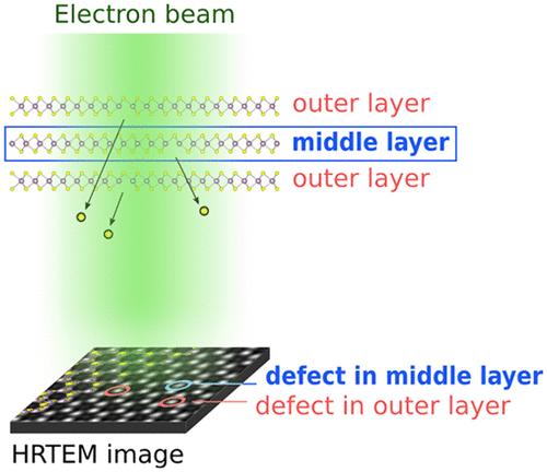
Defect Density and Atomic Defect Recognition in the Middle Layer of a Trilayer MoS2 Stack.
Molybdenum disulfide (MoS2) is one of the most intriguing two-dimensional materials, and moreover, its single atomic defects can significantly alter the properties. These defects can be both imaged and engineered using spherical and chromatic aberration-corrected high-resolution transmission electron microscopy (CC/CS-corrected HRTEM). In a few-layer stack, several atoms are vertically aligned in one atomic column. Therefore, it is challenging to determine the positions of missing atoms and the damage cross-section, particularly in the not directly accessible middle layers. In this study, we introduce a technique for extracting subtle intensity differences in CC/CS-corrected HRTEM images. By exploiting the crystal structure of the material, our method discerns chalcogen vacancies even in the middle layer of trilayer MoS2. We found that in trilayer MoS2 the middle layer's damage cross-section is about ten times lower than that in the monolayer. Our findings could be essential for the application of few-layer MoS2 in nanodevices.
期刊介绍:
Nano Letters serves as a dynamic platform for promptly disseminating original results in fundamental, applied, and emerging research across all facets of nanoscience and nanotechnology. A pivotal criterion for inclusion within Nano Letters is the convergence of at least two different areas or disciplines, ensuring a rich interdisciplinary scope. The journal is dedicated to fostering exploration in diverse areas, including:
- Experimental and theoretical findings on physical, chemical, and biological phenomena at the nanoscale
- Synthesis, characterization, and processing of organic, inorganic, polymer, and hybrid nanomaterials through physical, chemical, and biological methodologies
- Modeling and simulation of synthetic, assembly, and interaction processes
- Realization of integrated nanostructures and nano-engineered devices exhibiting advanced performance
- Applications of nanoscale materials in living and environmental systems
Nano Letters is committed to advancing and showcasing groundbreaking research that intersects various domains, fostering innovation and collaboration in the ever-evolving field of nanoscience and nanotechnology.


 分享
分享
 求助内容:
求助内容: 应助结果提醒方式:
 扫码关注我们
