Abin Varghese, Adityanarayan H. Pandey, Pooja Sharma, Yuefeng Yin, Nikhil V. Medhekar and Saurabh Lodha*,
{"title":"通过硅基板上的压电薄膜实现 MoS2 场效应晶体管中的电控高灵敏度应变调制。","authors":"Abin Varghese, Adityanarayan H. Pandey, Pooja Sharma, Yuefeng Yin, Nikhil V. Medhekar and Saurabh Lodha*, ","doi":"10.1021/acs.nanolett.4c00357","DOIUrl":null,"url":null,"abstract":"<p >Strain can modulate bandgap and carrier mobilities in two-dimensional (2D) materials. Conventional strain-application methodologies relying on flexible/patterned/nanoindented substrates are limited by low thermal tolerance, poor tunability, and/or scalability. Here, we leverage the converse piezoelectric effect to electrically generate and control strain transfer from a piezoelectric thin film to electromechanically coupled 2D MoS<sub>2</sub>. Electrical bias polarity change across the piezo film tunes the nature of strain transferred to MoS<sub>2</sub> from compressive (∼0.23%) to tensile (∼0.14%) as verified through Raman and photoluminescence spectroscopies and substantiated by density functional theory calculations. The device architecture, on silicon substrate, integrates an MoS<sub>2</sub> field-effect transistor on a metal-piezoelectric-metal stack enabling strain modulation of transistor drain current (130×), on/off ratio (150×), and mobility (1.19×) with high precision, reversibility, and resolution. Large, tunable tensile (1056) and compressive (−1498) strain gauge factors, electrical strain modulation, and high thermal tolerance promise facile integration with silicon-based CMOS and micro-electromechanical systems.</p>","PeriodicalId":53,"journal":{"name":"Nano Letters","volume":"24 28","pages":"8472–8480"},"PeriodicalIF":9.1000,"publicationDate":"2024-07-01","publicationTypes":"Journal Article","fieldsOfStudy":null,"isOpenAccess":false,"openAccessPdf":"","citationCount":"0","resultStr":"{\"title\":\"Electrically Controlled High Sensitivity Strain Modulation in MoS2 Field-Effect Transistors via a Piezoelectric Thin Film on Silicon Substrates\",\"authors\":\"Abin Varghese, Adityanarayan H. Pandey, Pooja Sharma, Yuefeng Yin, Nikhil V. Medhekar and Saurabh Lodha*, \",\"doi\":\"10.1021/acs.nanolett.4c00357\",\"DOIUrl\":null,\"url\":null,\"abstract\":\"<p >Strain can modulate bandgap and carrier mobilities in two-dimensional (2D) materials. Conventional strain-application methodologies relying on flexible/patterned/nanoindented substrates are limited by low thermal tolerance, poor tunability, and/or scalability. Here, we leverage the converse piezoelectric effect to electrically generate and control strain transfer from a piezoelectric thin film to electromechanically coupled 2D MoS<sub>2</sub>. Electrical bias polarity change across the piezo film tunes the nature of strain transferred to MoS<sub>2</sub> from compressive (∼0.23%) to tensile (∼0.14%) as verified through Raman and photoluminescence spectroscopies and substantiated by density functional theory calculations. The device architecture, on silicon substrate, integrates an MoS<sub>2</sub> field-effect transistor on a metal-piezoelectric-metal stack enabling strain modulation of transistor drain current (130×), on/off ratio (150×), and mobility (1.19×) with high precision, reversibility, and resolution. Large, tunable tensile (1056) and compressive (−1498) strain gauge factors, electrical strain modulation, and high thermal tolerance promise facile integration with silicon-based CMOS and micro-electromechanical systems.</p>\",\"PeriodicalId\":53,\"journal\":{\"name\":\"Nano Letters\",\"volume\":\"24 28\",\"pages\":\"8472–8480\"},\"PeriodicalIF\":9.1000,\"publicationDate\":\"2024-07-01\",\"publicationTypes\":\"Journal Article\",\"fieldsOfStudy\":null,\"isOpenAccess\":false,\"openAccessPdf\":\"\",\"citationCount\":\"0\",\"resultStr\":null,\"platform\":\"Semanticscholar\",\"paperid\":null,\"PeriodicalName\":\"Nano Letters\",\"FirstCategoryId\":\"88\",\"ListUrlMain\":\"https://pubs.acs.org/doi/10.1021/acs.nanolett.4c00357\",\"RegionNum\":1,\"RegionCategory\":\"材料科学\",\"ArticlePicture\":[],\"TitleCN\":null,\"AbstractTextCN\":null,\"PMCID\":null,\"EPubDate\":\"\",\"PubModel\":\"\",\"JCR\":\"Q1\",\"JCRName\":\"CHEMISTRY, MULTIDISCIPLINARY\",\"Score\":null,\"Total\":0}","platform":"Semanticscholar","paperid":null,"PeriodicalName":"Nano Letters","FirstCategoryId":"88","ListUrlMain":"https://pubs.acs.org/doi/10.1021/acs.nanolett.4c00357","RegionNum":1,"RegionCategory":"材料科学","ArticlePicture":[],"TitleCN":null,"AbstractTextCN":null,"PMCID":null,"EPubDate":"","PubModel":"","JCR":"Q1","JCRName":"CHEMISTRY, MULTIDISCIPLINARY","Score":null,"Total":0}
Electrically Controlled High Sensitivity Strain Modulation in MoS2 Field-Effect Transistors via a Piezoelectric Thin Film on Silicon Substrates
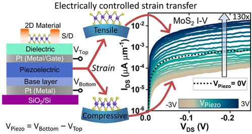
Strain can modulate bandgap and carrier mobilities in two-dimensional (2D) materials. Conventional strain-application methodologies relying on flexible/patterned/nanoindented substrates are limited by low thermal tolerance, poor tunability, and/or scalability. Here, we leverage the converse piezoelectric effect to electrically generate and control strain transfer from a piezoelectric thin film to electromechanically coupled 2D MoS2. Electrical bias polarity change across the piezo film tunes the nature of strain transferred to MoS2 from compressive (∼0.23%) to tensile (∼0.14%) as verified through Raman and photoluminescence spectroscopies and substantiated by density functional theory calculations. The device architecture, on silicon substrate, integrates an MoS2 field-effect transistor on a metal-piezoelectric-metal stack enabling strain modulation of transistor drain current (130×), on/off ratio (150×), and mobility (1.19×) with high precision, reversibility, and resolution. Large, tunable tensile (1056) and compressive (−1498) strain gauge factors, electrical strain modulation, and high thermal tolerance promise facile integration with silicon-based CMOS and micro-electromechanical systems.
期刊介绍:
Nano Letters serves as a dynamic platform for promptly disseminating original results in fundamental, applied, and emerging research across all facets of nanoscience and nanotechnology. A pivotal criterion for inclusion within Nano Letters is the convergence of at least two different areas or disciplines, ensuring a rich interdisciplinary scope. The journal is dedicated to fostering exploration in diverse areas, including:
- Experimental and theoretical findings on physical, chemical, and biological phenomena at the nanoscale
- Synthesis, characterization, and processing of organic, inorganic, polymer, and hybrid nanomaterials through physical, chemical, and biological methodologies
- Modeling and simulation of synthetic, assembly, and interaction processes
- Realization of integrated nanostructures and nano-engineered devices exhibiting advanced performance
- Applications of nanoscale materials in living and environmental systems
Nano Letters is committed to advancing and showcasing groundbreaking research that intersects various domains, fostering innovation and collaboration in the ever-evolving field of nanoscience and nanotechnology.


 分享
分享
 求助内容:
求助内容: 应助结果提醒方式:
 扫码关注我们
