Deborah Eric, Jianliang Jiang, Ali Imran and Abbas Ahmad Khan
{"title":"具有本征 GaN 夹层的 InxGa1-xN 量子点中间带太阳能电池的结构优化和工程设计","authors":"Deborah Eric, Jianliang Jiang, Ali Imran and Abbas Ahmad Khan","doi":"10.1039/D4YA00103F","DOIUrl":null,"url":null,"abstract":"<p >It is essential to have an adequately thick active layer to achieve efficient performance in quantum dot intermediate band solar cells (QD-IBSC) utilizing In<small><sub><em>x</em></sub></small>Ga<small><sub>1−<em>x</em></sub></small>N with high indium concentrations. The thickness plays a crucial role in maximizing photon absorption and optimizing the overall effectiveness of the solar cell (SC). In this paper, we introduce QD-IBSC with Ga-face (0 0 0 1) applying 1 nm i-GaN interlayers, which will provide strain relaxation to the In<small><sub>0.5</sub></small>Ga<small><sub>0.5</sub></small>N/GaN QD layer for increasing photovoltaic performance. Normally, the coupling among QDs splits the quantized energy level and leads to the formation of minibands within the forbidden region of conventional SC. In particular, the QDs are sensitive to dot regimentation and thus affect the properties of QD-IBSC. The electronic band structure of these QDs is controlled by changing the size of the QD, interdot distances and regimentation. In this paper, optimization of the optical structure of the QD-IBSC is performed by investigating the calculation results of both the maximum number of absorbed photons and the carrier transport property through tunneling simultaneously as a function of the thickness of the i-GaN interlayers. For the calculation, the three-dimensional regimented array of In<small><sub><em>x</em></sub></small>Ga<small><sub>1−<em>x</em></sub></small>N QD is analyzed using an envelope function. This work demonstrates Ga-face n–i–p structure (n-GaN/i-GaN:In<small><sub>0.5</sub></small>Ga<small><sub>0.5</sub></small>N:i-GaN/p-GaN) utilizing the 20 periods of 3 nm thick In<small><sub>0.5</sub></small>Ga<small><sub>0.5</sub></small>N QD layers and a GaN layer of 1 nm thickness can achieve a maximum conversion efficiency of 48%.</p>","PeriodicalId":72913,"journal":{"name":"Energy advances","volume":null,"pages":null},"PeriodicalIF":3.2000,"publicationDate":"2024-06-12","publicationTypes":"Journal Article","fieldsOfStudy":null,"isOpenAccess":false,"openAccessPdf":"https://pubs.rsc.org/en/content/articlepdf/2024/ya/d4ya00103f?page=search","citationCount":"0","resultStr":"{\"title\":\"Structural optimization and engineering of InxGa1−xN quantum dot intermediate band solar cells with intrinsic GaN interlayers\",\"authors\":\"Deborah Eric, Jianliang Jiang, Ali Imran and Abbas Ahmad Khan\",\"doi\":\"10.1039/D4YA00103F\",\"DOIUrl\":null,\"url\":null,\"abstract\":\"<p >It is essential to have an adequately thick active layer to achieve efficient performance in quantum dot intermediate band solar cells (QD-IBSC) utilizing In<small><sub><em>x</em></sub></small>Ga<small><sub>1−<em>x</em></sub></small>N with high indium concentrations. The thickness plays a crucial role in maximizing photon absorption and optimizing the overall effectiveness of the solar cell (SC). In this paper, we introduce QD-IBSC with Ga-face (0 0 0 1) applying 1 nm i-GaN interlayers, which will provide strain relaxation to the In<small><sub>0.5</sub></small>Ga<small><sub>0.5</sub></small>N/GaN QD layer for increasing photovoltaic performance. Normally, the coupling among QDs splits the quantized energy level and leads to the formation of minibands within the forbidden region of conventional SC. In particular, the QDs are sensitive to dot regimentation and thus affect the properties of QD-IBSC. The electronic band structure of these QDs is controlled by changing the size of the QD, interdot distances and regimentation. In this paper, optimization of the optical structure of the QD-IBSC is performed by investigating the calculation results of both the maximum number of absorbed photons and the carrier transport property through tunneling simultaneously as a function of the thickness of the i-GaN interlayers. For the calculation, the three-dimensional regimented array of In<small><sub><em>x</em></sub></small>Ga<small><sub>1−<em>x</em></sub></small>N QD is analyzed using an envelope function. This work demonstrates Ga-face n–i–p structure (n-GaN/i-GaN:In<small><sub>0.5</sub></small>Ga<small><sub>0.5</sub></small>N:i-GaN/p-GaN) utilizing the 20 periods of 3 nm thick In<small><sub>0.5</sub></small>Ga<small><sub>0.5</sub></small>N QD layers and a GaN layer of 1 nm thickness can achieve a maximum conversion efficiency of 48%.</p>\",\"PeriodicalId\":72913,\"journal\":{\"name\":\"Energy advances\",\"volume\":null,\"pages\":null},\"PeriodicalIF\":3.2000,\"publicationDate\":\"2024-06-12\",\"publicationTypes\":\"Journal Article\",\"fieldsOfStudy\":null,\"isOpenAccess\":false,\"openAccessPdf\":\"https://pubs.rsc.org/en/content/articlepdf/2024/ya/d4ya00103f?page=search\",\"citationCount\":\"0\",\"resultStr\":null,\"platform\":\"Semanticscholar\",\"paperid\":null,\"PeriodicalName\":\"Energy advances\",\"FirstCategoryId\":\"1085\",\"ListUrlMain\":\"https://pubs.rsc.org/en/content/articlelanding/2024/ya/d4ya00103f\",\"RegionNum\":0,\"RegionCategory\":null,\"ArticlePicture\":[],\"TitleCN\":null,\"AbstractTextCN\":null,\"PMCID\":null,\"EPubDate\":\"\",\"PubModel\":\"\",\"JCR\":\"Q2\",\"JCRName\":\"CHEMISTRY, PHYSICAL\",\"Score\":null,\"Total\":0}","platform":"Semanticscholar","paperid":null,"PeriodicalName":"Energy advances","FirstCategoryId":"1085","ListUrlMain":"https://pubs.rsc.org/en/content/articlelanding/2024/ya/d4ya00103f","RegionNum":0,"RegionCategory":null,"ArticlePicture":[],"TitleCN":null,"AbstractTextCN":null,"PMCID":null,"EPubDate":"","PubModel":"","JCR":"Q2","JCRName":"CHEMISTRY, PHYSICAL","Score":null,"Total":0}
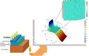
Structural optimization and engineering of InxGa1−xN quantum dot intermediate band solar cells with intrinsic GaN interlayers
It is essential to have an adequately thick active layer to achieve efficient performance in quantum dot intermediate band solar cells (QD-IBSC) utilizing InxGa1−xN with high indium concentrations. The thickness plays a crucial role in maximizing photon absorption and optimizing the overall effectiveness of the solar cell (SC). In this paper, we introduce QD-IBSC with Ga-face (0 0 0 1) applying 1 nm i-GaN interlayers, which will provide strain relaxation to the In0.5Ga0.5N/GaN QD layer for increasing photovoltaic performance. Normally, the coupling among QDs splits the quantized energy level and leads to the formation of minibands within the forbidden region of conventional SC. In particular, the QDs are sensitive to dot regimentation and thus affect the properties of QD-IBSC. The electronic band structure of these QDs is controlled by changing the size of the QD, interdot distances and regimentation. In this paper, optimization of the optical structure of the QD-IBSC is performed by investigating the calculation results of both the maximum number of absorbed photons and the carrier transport property through tunneling simultaneously as a function of the thickness of the i-GaN interlayers. For the calculation, the three-dimensional regimented array of InxGa1−xN QD is analyzed using an envelope function. This work demonstrates Ga-face n–i–p structure (n-GaN/i-GaN:In0.5Ga0.5N:i-GaN/p-GaN) utilizing the 20 periods of 3 nm thick In0.5Ga0.5N QD layers and a GaN layer of 1 nm thickness can achieve a maximum conversion efficiency of 48%.


 分享
分享

 求助内容:
求助内容: 应助结果提醒方式:
 扫码关注我们
