Salah M. Abdul Aziz, Uday M. Nayef, Mohammed Rasheed
{"title":"在液体中通过激光烧蚀合成纳米氧化铜颗粒以增强光谱响应性","authors":"Salah M. Abdul Aziz, Uday M. Nayef, Mohammed Rasheed","doi":"10.1007/s11468-024-02472-5","DOIUrl":null,"url":null,"abstract":"<div><p>This research included the production of copper oxide nanoparticles (CuO NPs) using various pulsed laser ablation energy (PLAL) embedded in substrates made of porous silicon (PS). The PS substrates were created using the photoelectrochemical etching (PECE) technique of Si n-type (111). The research examined the impact of pulse laser ablation energy on many attributes of the created samples, involving their structural, electrical, optical, photodetector, and morphological properties. XRD analysis reveals a prominent and broad diffraction peak at an angle of 28.4<sup>ο</sup> for the porous silicon and other diffraction peaks at different angles, indicating the presence of the CuO NPs phase corresponding to the monoclinic crystal structure. The SEM image demonstrates that PS is sponge-like, while CuO NPs display randomly dispersed spherical grains, and appear to vary in the particle size due to the change in laser pulses energy. </p><p>The optical properties of the fabricated specimens were analyzed utilizing photoluminescence and UV–vis absorption spectroscopy. The results suggested that a change in laser pulse energy caused a change in the energy gap that ranges from 2.7 to 3.5 eV. The created samples' current density-voltage (J-V) characteristics were analyzed under two conditions: in dark and light while varying the laser pulse energy. The J-V characteristics curves demonstrate that increasing the pulse energies of laser ablation resulted in higher current density flowing through the samples, particularly when the sample was created at 900 mJ. The photocurrent density exhibited a significant association with the increase in input light intensity, so enabling its utilization as a photodetector device. Nevertheless, altering the laser ablation pulse energy resulted in modifying the photocurrent for all CuO NPs/PS specimens. The inclusion of CuO nanoparticles in the PS samples led to a considerable enhancement in the responsivity (Rλ) when compared to the PS-only sample. The reason for this is that CuO nanoparticles have the ability to absorb light throughout a wide range of wavelengths, from ultraviolet-visible to near-infrared. The highest detectivity (D*) value was recorded when the laser energy was set at 700 mJ. The observed phenomena can be ascribed to fluctuations in the size or morphology of CuO NPs caused by variations in laser ablation pulse energy during its preparation. Furthermore, the constructed photodetector exhibited enhanced external quantum efficiency (Q.E), specifically in the ultraviolet (UV) range. The findings of this research are significant in the progress of optoelectronic and photodetector devices that rely on CuO NPs and PS.</p></div>","PeriodicalId":736,"journal":{"name":"Plasmonics","volume":"20 5","pages":"2869 - 2879"},"PeriodicalIF":4.3000,"publicationDate":"2024-08-31","publicationTypes":"Journal Article","fieldsOfStudy":null,"isOpenAccess":false,"openAccessPdf":"","citationCount":"0","resultStr":"{\"title\":\"Synthesis of Copper Oxide Nanoparticles via Laser Ablation in Liquid for Enhancing Spectral Responsivity\",\"authors\":\"Salah M. Abdul Aziz, Uday M. Nayef, Mohammed Rasheed\",\"doi\":\"10.1007/s11468-024-02472-5\",\"DOIUrl\":null,\"url\":null,\"abstract\":\"<div><p>This research included the production of copper oxide nanoparticles (CuO NPs) using various pulsed laser ablation energy (PLAL) embedded in substrates made of porous silicon (PS). The PS substrates were created using the photoelectrochemical etching (PECE) technique of Si n-type (111). The research examined the impact of pulse laser ablation energy on many attributes of the created samples, involving their structural, electrical, optical, photodetector, and morphological properties. XRD analysis reveals a prominent and broad diffraction peak at an angle of 28.4<sup>ο</sup> for the porous silicon and other diffraction peaks at different angles, indicating the presence of the CuO NPs phase corresponding to the monoclinic crystal structure. The SEM image demonstrates that PS is sponge-like, while CuO NPs display randomly dispersed spherical grains, and appear to vary in the particle size due to the change in laser pulses energy. </p><p>The optical properties of the fabricated specimens were analyzed utilizing photoluminescence and UV–vis absorption spectroscopy. The results suggested that a change in laser pulse energy caused a change in the energy gap that ranges from 2.7 to 3.5 eV. The created samples' current density-voltage (J-V) characteristics were analyzed under two conditions: in dark and light while varying the laser pulse energy. The J-V characteristics curves demonstrate that increasing the pulse energies of laser ablation resulted in higher current density flowing through the samples, particularly when the sample was created at 900 mJ. The photocurrent density exhibited a significant association with the increase in input light intensity, so enabling its utilization as a photodetector device. Nevertheless, altering the laser ablation pulse energy resulted in modifying the photocurrent for all CuO NPs/PS specimens. The inclusion of CuO nanoparticles in the PS samples led to a considerable enhancement in the responsivity (Rλ) when compared to the PS-only sample. The reason for this is that CuO nanoparticles have the ability to absorb light throughout a wide range of wavelengths, from ultraviolet-visible to near-infrared. The highest detectivity (D*) value was recorded when the laser energy was set at 700 mJ. The observed phenomena can be ascribed to fluctuations in the size or morphology of CuO NPs caused by variations in laser ablation pulse energy during its preparation. Furthermore, the constructed photodetector exhibited enhanced external quantum efficiency (Q.E), specifically in the ultraviolet (UV) range. The findings of this research are significant in the progress of optoelectronic and photodetector devices that rely on CuO NPs and PS.</p></div>\",\"PeriodicalId\":736,\"journal\":{\"name\":\"Plasmonics\",\"volume\":\"20 5\",\"pages\":\"2869 - 2879\"},\"PeriodicalIF\":4.3000,\"publicationDate\":\"2024-08-31\",\"publicationTypes\":\"Journal Article\",\"fieldsOfStudy\":null,\"isOpenAccess\":false,\"openAccessPdf\":\"\",\"citationCount\":\"0\",\"resultStr\":null,\"platform\":\"Semanticscholar\",\"paperid\":null,\"PeriodicalName\":\"Plasmonics\",\"FirstCategoryId\":\"101\",\"ListUrlMain\":\"https://link.springer.com/article/10.1007/s11468-024-02472-5\",\"RegionNum\":4,\"RegionCategory\":\"物理与天体物理\",\"ArticlePicture\":[],\"TitleCN\":null,\"AbstractTextCN\":null,\"PMCID\":null,\"EPubDate\":\"\",\"PubModel\":\"\",\"JCR\":\"Q2\",\"JCRName\":\"CHEMISTRY, PHYSICAL\",\"Score\":null,\"Total\":0}","platform":"Semanticscholar","paperid":null,"PeriodicalName":"Plasmonics","FirstCategoryId":"101","ListUrlMain":"https://link.springer.com/article/10.1007/s11468-024-02472-5","RegionNum":4,"RegionCategory":"物理与天体物理","ArticlePicture":[],"TitleCN":null,"AbstractTextCN":null,"PMCID":null,"EPubDate":"","PubModel":"","JCR":"Q2","JCRName":"CHEMISTRY, PHYSICAL","Score":null,"Total":0}
Synthesis of Copper Oxide Nanoparticles via Laser Ablation in Liquid for Enhancing Spectral Responsivity
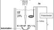
This research included the production of copper oxide nanoparticles (CuO NPs) using various pulsed laser ablation energy (PLAL) embedded in substrates made of porous silicon (PS). The PS substrates were created using the photoelectrochemical etching (PECE) technique of Si n-type (111). The research examined the impact of pulse laser ablation energy on many attributes of the created samples, involving their structural, electrical, optical, photodetector, and morphological properties. XRD analysis reveals a prominent and broad diffraction peak at an angle of 28.4ο for the porous silicon and other diffraction peaks at different angles, indicating the presence of the CuO NPs phase corresponding to the monoclinic crystal structure. The SEM image demonstrates that PS is sponge-like, while CuO NPs display randomly dispersed spherical grains, and appear to vary in the particle size due to the change in laser pulses energy.
The optical properties of the fabricated specimens were analyzed utilizing photoluminescence and UV–vis absorption spectroscopy. The results suggested that a change in laser pulse energy caused a change in the energy gap that ranges from 2.7 to 3.5 eV. The created samples' current density-voltage (J-V) characteristics were analyzed under two conditions: in dark and light while varying the laser pulse energy. The J-V characteristics curves demonstrate that increasing the pulse energies of laser ablation resulted in higher current density flowing through the samples, particularly when the sample was created at 900 mJ. The photocurrent density exhibited a significant association with the increase in input light intensity, so enabling its utilization as a photodetector device. Nevertheless, altering the laser ablation pulse energy resulted in modifying the photocurrent for all CuO NPs/PS specimens. The inclusion of CuO nanoparticles in the PS samples led to a considerable enhancement in the responsivity (Rλ) when compared to the PS-only sample. The reason for this is that CuO nanoparticles have the ability to absorb light throughout a wide range of wavelengths, from ultraviolet-visible to near-infrared. The highest detectivity (D*) value was recorded when the laser energy was set at 700 mJ. The observed phenomena can be ascribed to fluctuations in the size or morphology of CuO NPs caused by variations in laser ablation pulse energy during its preparation. Furthermore, the constructed photodetector exhibited enhanced external quantum efficiency (Q.E), specifically in the ultraviolet (UV) range. The findings of this research are significant in the progress of optoelectronic and photodetector devices that rely on CuO NPs and PS.
期刊介绍:
Plasmonics is an international forum for the publication of peer-reviewed leading-edge original articles that both advance and report our knowledge base and practice of the interactions of free-metal electrons, Plasmons.
Topics covered include notable advances in the theory, Physics, and applications of surface plasmons in metals, to the rapidly emerging areas of nanotechnology, biophotonics, sensing, biochemistry and medicine. Topics, including the theory, synthesis and optical properties of noble metal nanostructures, patterned surfaces or materials, continuous or grated surfaces, devices, or wires for their multifarious applications are particularly welcome. Typical applications might include but are not limited to, surface enhanced spectroscopic properties, such as Raman scattering or fluorescence, as well developments in techniques such as surface plasmon resonance and near-field scanning optical microscopy.


 分享
分享
 求助内容:
求助内容: 应助结果提醒方式:
 扫码关注我们
