Tingkai Xu, Qihang Lv, Xuyang Li, Zitong Xu, Wang Xin, Xia Shen, Pengfei Guo* and Liantuan Xiao,
{"title":"CdS/Sn超晶格纳米线的形成与室温微腔激发发射","authors":"Tingkai Xu, Qihang Lv, Xuyang Li, Zitong Xu, Wang Xin, Xia Shen, Pengfei Guo* and Liantuan Xiao, ","doi":"10.1021/acsanm.5c00587","DOIUrl":null,"url":null,"abstract":"<p >Semiconductor superlattice nanowires are promising candidates for multifunctional optoelectronic devices due to their periodic structure and compositional modulation. However, the realization of superlattice nanowires for multiple microcavity nanolasers remains challenging. Here, we report a rational strategy for the synthesis of CdS/Sn superlattice nanowires by a chemical vapor deposition (CVD) approach. Structural characterization reveals periodic CdS and Sn segments along the nanowire axis. Spatially resolved microphotoluminescence measurements confirm multiple microcavities between the adjacent Sn nodes in a single nanowire. Additionally, a room-temperature single-mode laser is clearly observed from these superlattice nanowires, which shows a strong stimulated emission with a high-quality factor (∼1218). These findings suggest that the prepared CdS/Sn superlattice nanowires provide a versatile platform for light–matter interaction studies and can be used as an excellent optical gain medium for high-quality factor lasers.</p>","PeriodicalId":6,"journal":{"name":"ACS Applied Nano Materials","volume":"8 14","pages":"7235–7242 7235–7242"},"PeriodicalIF":5.8000,"publicationDate":"2025-03-31","publicationTypes":"Journal Article","fieldsOfStudy":null,"isOpenAccess":false,"openAccessPdf":"","citationCount":"0","resultStr":"{\"title\":\"Formation of CdS/Sn Superlattice Nanowires and Room-Temperature Microcavity Stimulated Emission\",\"authors\":\"Tingkai Xu, Qihang Lv, Xuyang Li, Zitong Xu, Wang Xin, Xia Shen, Pengfei Guo* and Liantuan Xiao, \",\"doi\":\"10.1021/acsanm.5c00587\",\"DOIUrl\":null,\"url\":null,\"abstract\":\"<p >Semiconductor superlattice nanowires are promising candidates for multifunctional optoelectronic devices due to their periodic structure and compositional modulation. However, the realization of superlattice nanowires for multiple microcavity nanolasers remains challenging. Here, we report a rational strategy for the synthesis of CdS/Sn superlattice nanowires by a chemical vapor deposition (CVD) approach. Structural characterization reveals periodic CdS and Sn segments along the nanowire axis. Spatially resolved microphotoluminescence measurements confirm multiple microcavities between the adjacent Sn nodes in a single nanowire. Additionally, a room-temperature single-mode laser is clearly observed from these superlattice nanowires, which shows a strong stimulated emission with a high-quality factor (∼1218). These findings suggest that the prepared CdS/Sn superlattice nanowires provide a versatile platform for light–matter interaction studies and can be used as an excellent optical gain medium for high-quality factor lasers.</p>\",\"PeriodicalId\":6,\"journal\":{\"name\":\"ACS Applied Nano Materials\",\"volume\":\"8 14\",\"pages\":\"7235–7242 7235–7242\"},\"PeriodicalIF\":5.8000,\"publicationDate\":\"2025-03-31\",\"publicationTypes\":\"Journal Article\",\"fieldsOfStudy\":null,\"isOpenAccess\":false,\"openAccessPdf\":\"\",\"citationCount\":\"0\",\"resultStr\":null,\"platform\":\"Semanticscholar\",\"paperid\":null,\"PeriodicalName\":\"ACS Applied Nano Materials\",\"FirstCategoryId\":\"88\",\"ListUrlMain\":\"https://pubs.acs.org/doi/10.1021/acsanm.5c00587\",\"RegionNum\":2,\"RegionCategory\":\"材料科学\",\"ArticlePicture\":[],\"TitleCN\":null,\"AbstractTextCN\":null,\"PMCID\":null,\"EPubDate\":\"\",\"PubModel\":\"\",\"JCR\":\"Q2\",\"JCRName\":\"MATERIALS SCIENCE, MULTIDISCIPLINARY\",\"Score\":null,\"Total\":0}","platform":"Semanticscholar","paperid":null,"PeriodicalName":"ACS Applied Nano Materials","FirstCategoryId":"88","ListUrlMain":"https://pubs.acs.org/doi/10.1021/acsanm.5c00587","RegionNum":2,"RegionCategory":"材料科学","ArticlePicture":[],"TitleCN":null,"AbstractTextCN":null,"PMCID":null,"EPubDate":"","PubModel":"","JCR":"Q2","JCRName":"MATERIALS SCIENCE, MULTIDISCIPLINARY","Score":null,"Total":0}
引用次数: 0
摘要
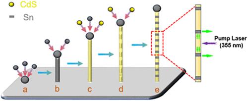
半导体超晶格纳米线具有周期性结构和成分调制特性,是多功能光电器件的理想候选材料。然而,实现用于多微腔纳米激光器的超晶格纳米线仍然具有挑战性。在此,我们报告了一种通过化学气相沉积(CVD)方法合成 CdS/Sn 超晶格纳米线的合理策略。结构表征显示了沿纳米线轴线的周期性 CdS 和 Sn 段。空间分辨微光致发光测量证实了单根纳米线中相邻锡节点之间存在多个微腔。此外,还能从这些超晶格纳米线上清晰地观察到室温单模激光,其高质量系数(1218)显示出强烈的受激发射。这些发现表明,所制备的 CdS/Sn 超晶格纳米线为光-物质相互作用研究提供了一个多功能平台,并可用作高质量因子激光器的优良光学增益介质。
Formation of CdS/Sn Superlattice Nanowires and Room-Temperature Microcavity Stimulated Emission
Semiconductor superlattice nanowires are promising candidates for multifunctional optoelectronic devices due to their periodic structure and compositional modulation. However, the realization of superlattice nanowires for multiple microcavity nanolasers remains challenging. Here, we report a rational strategy for the synthesis of CdS/Sn superlattice nanowires by a chemical vapor deposition (CVD) approach. Structural characterization reveals periodic CdS and Sn segments along the nanowire axis. Spatially resolved microphotoluminescence measurements confirm multiple microcavities between the adjacent Sn nodes in a single nanowire. Additionally, a room-temperature single-mode laser is clearly observed from these superlattice nanowires, which shows a strong stimulated emission with a high-quality factor (∼1218). These findings suggest that the prepared CdS/Sn superlattice nanowires provide a versatile platform for light–matter interaction studies and can be used as an excellent optical gain medium for high-quality factor lasers.
期刊介绍:
ACS Applied Nano Materials is an interdisciplinary journal publishing original research covering all aspects of engineering, chemistry, physics and biology relevant to applications of nanomaterials. The journal is devoted to reports of new and original experimental and theoretical research of an applied nature that integrate knowledge in the areas of materials, engineering, physics, bioscience, and chemistry into important applications of nanomaterials.


 分享
分享
 求助内容:
求助内容: 应助结果提醒方式:
 扫码关注我们
