Yuhang Li , Zhe Zhang , Qi Song , Haiyan Shi , Yu Hou , Song Yue , Ran Wang , Shunshuo Cai , Zichen Zhang
{"title":"Surface micromorphology and nanostructures evolution in hybrid laser processes of slicing and polishing single crystal 4H-SiC","authors":"Yuhang Li , Zhe Zhang , Qi Song , Haiyan Shi , Yu Hou , Song Yue , Ran Wang , Shunshuo Cai , Zichen Zhang","doi":"10.1016/j.jmst.2023.09.046","DOIUrl":null,"url":null,"abstract":"<div><p><span>Slicing and post-treatment of SiC crystals have been a significant challenge in the integrated circuit and microelectronics industry. To compete with wire-sawing and mechanical grinding technology, a promising approach combining laser slicing and laser polishing technologies has been innovatively applied to increase utilization and decrease damage defects for single crystal 4H-SiC. Significant material utilization has been achieved in the hybrid laser processes, where material loss is reduced by 75% compared to that of conventional machining technologies. Without any special process control or additional treatment, an internally modified layer formed by laser slicing can easily separate the 4H-SiC crystals using an external force of about ∼3.6 MPa. The modified layer has been characterized using a micro-Raman method to determine residual stress. The sliced surface exhibits a combination of smooth and coarse appearances around the fluvial morphology, with an average surface roughness of over </span><em>S</em><sub>a</sub> 0.89 µm. An amorphous phase surrounds the SiC substrate, with two dimensions of lattice spacing, <em>d</em> = 0.261 nm and <em>d</em> = 0.265 nm, confirmed by high-resolution transmission electron microscopy (HRTEM). The creation of laser-induced periodic surface nanostructures in the laser-polished surface results in a flatter surface with an average roughness of less than <em>S</em><sub>a</sub> 0.22 µm. Due to the extreme cooling rates and multiple thermal cycles, dissociation of Si-C bonding, and phase separation are identified on the laser-polished surface, which is much better than that of the machining surface. We anticipate that this approach will be applicable to other high-value crystals and will have promising viability in the aerospace and semiconductor industries.</p></div>","PeriodicalId":16154,"journal":{"name":"Journal of Materials Science & Technology","volume":"184 ","pages":"Pages 235-244"},"PeriodicalIF":14.3000,"publicationDate":"2024-06-10","publicationTypes":"Journal Article","fieldsOfStudy":null,"isOpenAccess":false,"openAccessPdf":"","citationCount":"0","resultStr":null,"platform":"Semanticscholar","paperid":null,"PeriodicalName":"Journal of Materials Science & Technology","FirstCategoryId":"1087","ListUrlMain":"https://www.sciencedirect.com/science/article/pii/S1005030223009209","RegionNum":1,"RegionCategory":"材料科学","ArticlePicture":[],"TitleCN":null,"AbstractTextCN":null,"PMCID":null,"EPubDate":"2023/11/23 0:00:00","PubModel":"Epub","JCR":"Q1","JCRName":"MATERIALS SCIENCE, MULTIDISCIPLINARY","Score":null,"Total":0}
引用次数: 0
Abstract
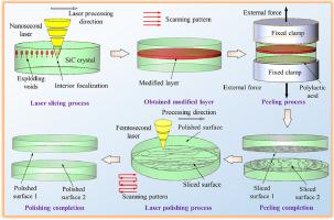
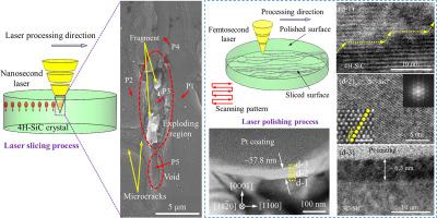
Slicing and post-treatment of SiC crystals have been a significant challenge in the integrated circuit and microelectronics industry. To compete with wire-sawing and mechanical grinding technology, a promising approach combining laser slicing and laser polishing technologies has been innovatively applied to increase utilization and decrease damage defects for single crystal 4H-SiC. Significant material utilization has been achieved in the hybrid laser processes, where material loss is reduced by 75% compared to that of conventional machining technologies. Without any special process control or additional treatment, an internally modified layer formed by laser slicing can easily separate the 4H-SiC crystals using an external force of about ∼3.6 MPa. The modified layer has been characterized using a micro-Raman method to determine residual stress. The sliced surface exhibits a combination of smooth and coarse appearances around the fluvial morphology, with an average surface roughness of over Sa 0.89 µm. An amorphous phase surrounds the SiC substrate, with two dimensions of lattice spacing, d = 0.261 nm and d = 0.265 nm, confirmed by high-resolution transmission electron microscopy (HRTEM). The creation of laser-induced periodic surface nanostructures in the laser-polished surface results in a flatter surface with an average roughness of less than Sa 0.22 µm. Due to the extreme cooling rates and multiple thermal cycles, dissociation of Si-C bonding, and phase separation are identified on the laser-polished surface, which is much better than that of the machining surface. We anticipate that this approach will be applicable to other high-value crystals and will have promising viability in the aerospace and semiconductor industries.
期刊介绍:
Journal of Materials Science & Technology strives to promote global collaboration in the field of materials science and technology. It primarily publishes original research papers, invited review articles, letters, research notes, and summaries of scientific achievements. The journal covers a wide range of materials science and technology topics, including metallic materials, inorganic nonmetallic materials, and composite materials.


 分享
分享
 求助内容:
求助内容: 应助结果提醒方式:
 扫码关注我们
