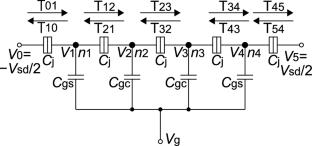
{"title":"Arrangement rule of stability regions and single-electron transfer in common-gate quadruple-dot devices for the real ratio of gate capacitances","authors":"Shigeru Imai, Yusuke Watanabe","doi":"10.1007/s10825-023-02119-4","DOIUrl":null,"url":null,"abstract":"<div><p>For single-electron transfer in common-gate multidot devices, the arrangement of stability regions along the gate voltage (<i>V</i><sub>g</sub>) axis is important because single-electron transfer occurs around the overlap of stability regions. The stability regions along the <i>V</i><sub>g</sub> axis are well known to have periodicity when the device has an integer ratio of gate capacitances (<i>C</i><sub>g</sub>). However, the arrangement rule for the real <i>C</i><sub>g</sub> ratio is unclear. In this paper, stability regions for quadruple-dot devices with symmetric <i>C</i><sub>g</sub> are exhaustively examined. The arrangement of stability regions along the <i>V</i><sub>g</sub> axis is drawn as a map of the real <i>C</i><sub>g</sub> ratio in a newly proposed diagram. Here, the arrangement for a particular <i>C</i><sub>g</sub> ratio is drawn along a straight line that passes through the origin and has a slope depending on the <i>C</i><sub>g</sub> ratio. In the diagram, stability regions are arranged two-dimensionally, and the abovementioned periodicity for integer <i>C</i><sub>g</sub> ratios clearly appears. How neighboring stability regions interrelate with each other in the diagram is mathematically examined and described in detail. Next, the sequences of tunneling events around the overlap of stability regions are investigated, and eight kinds of tunneling sequences for single-electron transfer are determined.</p></div>","PeriodicalId":620,"journal":{"name":"Journal of Computational Electronics","volume":"23 1","pages":"51 - 64"},"PeriodicalIF":2.5000,"publicationDate":"2024-01-04","publicationTypes":"Journal Article","fieldsOfStudy":null,"isOpenAccess":false,"openAccessPdf":"","citationCount":"0","resultStr":null,"platform":"Semanticscholar","paperid":null,"PeriodicalName":"Journal of Computational Electronics","FirstCategoryId":"5","ListUrlMain":"https://link.springer.com/article/10.1007/s10825-023-02119-4","RegionNum":4,"RegionCategory":"工程技术","ArticlePicture":[],"TitleCN":null,"AbstractTextCN":null,"PMCID":null,"EPubDate":"","PubModel":"","JCR":"Q3","JCRName":"ENGINEERING, ELECTRICAL & ELECTRONIC","Score":null,"Total":0}
引用次数: 0
Abstract
For single-electron transfer in common-gate multidot devices, the arrangement of stability regions along the gate voltage (Vg) axis is important because single-electron transfer occurs around the overlap of stability regions. The stability regions along the Vg axis are well known to have periodicity when the device has an integer ratio of gate capacitances (Cg). However, the arrangement rule for the real Cg ratio is unclear. In this paper, stability regions for quadruple-dot devices with symmetric Cg are exhaustively examined. The arrangement of stability regions along the Vg axis is drawn as a map of the real Cg ratio in a newly proposed diagram. Here, the arrangement for a particular Cg ratio is drawn along a straight line that passes through the origin and has a slope depending on the Cg ratio. In the diagram, stability regions are arranged two-dimensionally, and the abovementioned periodicity for integer Cg ratios clearly appears. How neighboring stability regions interrelate with each other in the diagram is mathematically examined and described in detail. Next, the sequences of tunneling events around the overlap of stability regions are investigated, and eight kinds of tunneling sequences for single-electron transfer are determined.
期刊介绍:
he Journal of Computational Electronics brings together research on all aspects of modeling and simulation of modern electronics. This includes optical, electronic, mechanical, and quantum mechanical aspects, as well as research on the underlying mathematical algorithms and computational details. The related areas of energy conversion/storage and of molecular and biological systems, in which the thrust is on the charge transport, electronic, mechanical, and optical properties, are also covered.
In particular, we encourage manuscripts dealing with device simulation; with optical and optoelectronic systems and photonics; with energy storage (e.g. batteries, fuel cells) and harvesting (e.g. photovoltaic), with simulation of circuits, VLSI layout, logic and architecture (based on, for example, CMOS devices, quantum-cellular automata, QBITs, or single-electron transistors); with electromagnetic simulations (such as microwave electronics and components); or with molecular and biological systems. However, in all these cases, the submitted manuscripts should explicitly address the electronic properties of the relevant systems, materials, or devices and/or present novel contributions to the physical models, computational strategies, or numerical algorithms.


 分享
分享
 求助内容:
求助内容: 应助结果提醒方式:
 扫码关注我们
