Jean-Philippe Soulié , Kiroubanand Sankaran , Valeria Founta , Karl Opsomer , Christophe Detavernier , Joris Van de Vondel , Geoffrey Pourtois , Zsolt Tőkei , Johan Swerts , Christoph Adelmann
{"title":"Al3Sc thin films for advanced interconnect applications","authors":"Jean-Philippe Soulié , Kiroubanand Sankaran , Valeria Founta , Karl Opsomer , Christophe Detavernier , Joris Van de Vondel , Geoffrey Pourtois , Zsolt Tőkei , Johan Swerts , Christoph Adelmann","doi":"10.1016/j.mee.2024.112141","DOIUrl":null,"url":null,"abstract":"<div><p>Al<sub><em>x</em></sub>Sc<sub><em>1-x</em></sub><span> thin films have been studied with compositions around Al</span><sub>3</sub>Sc (<em>x</em><span> = 0.75) for potential interconnect metallization<span> applications. As-deposited 25 nm thick films<span> were x-ray amorphous but crystallized at 190 °C, followed by recrystallization at 440 °C. After annealing at 500 °C, 24 nm thick stoichiometric Al</span></span></span><sub>3</sub><span>Sc showed a resistivity of 12.6 μΩcm, limited by a combination of grain boundary and point defect (disorder) scattering. Together with </span><em>ab initio</em><span> calculations that found a mean free path of the charge carriers of 7 nm for stoichiometric Al</span><sub>3</sub>Sc, these results indicate that Al<sub>3</sub><span><span>Sc bears promise for future interconnect metallization schemes. Challenges remain in minimizing the formation of secondary phases as well as in the control of the non-stoichiometric surface oxidation and interfacial reactions with underlying </span>dielectrics.</span></p></div>","PeriodicalId":18557,"journal":{"name":"Microelectronic Engineering","volume":"286 ","pages":"Article 112141"},"PeriodicalIF":3.1000,"publicationDate":"2024-03-01","publicationTypes":"Journal Article","fieldsOfStudy":null,"isOpenAccess":false,"openAccessPdf":"","citationCount":"0","resultStr":null,"platform":"Semanticscholar","paperid":null,"PeriodicalName":"Microelectronic Engineering","FirstCategoryId":"5","ListUrlMain":"https://www.sciencedirect.com/science/article/pii/S0167931724000108","RegionNum":4,"RegionCategory":"工程技术","ArticlePicture":[],"TitleCN":null,"AbstractTextCN":null,"PMCID":null,"EPubDate":"2024/1/23 0:00:00","PubModel":"Epub","JCR":"Q2","JCRName":"ENGINEERING, ELECTRICAL & ELECTRONIC","Score":null,"Total":0}
引用次数: 0
Abstract
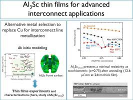
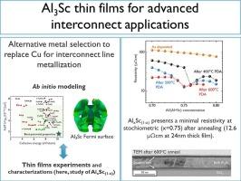
AlxSc1-x thin films have been studied with compositions around Al3Sc (x = 0.75) for potential interconnect metallization applications. As-deposited 25 nm thick films were x-ray amorphous but crystallized at 190 °C, followed by recrystallization at 440 °C. After annealing at 500 °C, 24 nm thick stoichiometric Al3Sc showed a resistivity of 12.6 μΩcm, limited by a combination of grain boundary and point defect (disorder) scattering. Together with ab initio calculations that found a mean free path of the charge carriers of 7 nm for stoichiometric Al3Sc, these results indicate that Al3Sc bears promise for future interconnect metallization schemes. Challenges remain in minimizing the formation of secondary phases as well as in the control of the non-stoichiometric surface oxidation and interfacial reactions with underlying dielectrics.
期刊介绍:
Microelectronic Engineering is the premier nanoprocessing, and nanotechnology journal focusing on fabrication of electronic, photonic, bioelectronic, electromechanic and fluidic devices and systems, and their applications in the broad areas of electronics, photonics, energy, life sciences, and environment. It covers also the expanding interdisciplinary field of "more than Moore" and "beyond Moore" integrated nanoelectronics / photonics and micro-/nano-/bio-systems. Through its unique mixture of peer-reviewed articles, reviews, accelerated publications, short and Technical notes, and the latest research news on key developments, Microelectronic Engineering provides comprehensive coverage of this exciting, interdisciplinary and dynamic new field for researchers in academia and professionals in industry.


 分享
分享
 求助内容:
求助内容: 应助结果提醒方式:
 扫码关注我们
