Jordan Athas , Joseph Ereifej , Jorge Torres Quiñones, Alexander Abrams, Minhee Yun
{"title":"A scalable top-gate graphene field effect transistor with a polydimethylsiloxane dielectric","authors":"Jordan Athas , Joseph Ereifej , Jorge Torres Quiñones, Alexander Abrams, Minhee Yun","doi":"10.1016/j.nwnano.2024.100039","DOIUrl":null,"url":null,"abstract":"<div><p>The limitations of modern CMOS technology have created a call to action for novel devices with great scalability potential. Graphene has been recognized as a suitable material for an enhanced transistor channel based on its incredibly large conductivity while also being easily scaled. Previous research has noted the importance of a top gate device structure, which is difficult to accomplish for graphene transistors due to graphene's incompatibility with oxide growth processes. A novel process flow for graphene field effect transistors with scalability is presented. The emphasis is on the growth of multilayer graphene using chemical vapor deposition and the implementation of polydimethylsiloxane as a gate dielectric. Polydimethylsiloxane gate insulator thickness of 815 nm and 570 nm were successfully developed on 4in large-scale wafers. Two devices of similar channel dimensions and different dielectric were compared and mobilities of 14.57cm<sup>2</sup>V<sup>−1</sup>s<sup>−1</sup> and 0.44 cm<sup>2</sup>V<sup>−1</sup>s<sup>−1</sup> were measured. Gate voltage sweeps from -20 V to 20 V also demonstrated channel current modulation with a charge neutrality point between 5 V and 8 V, indicating achievement of expected device operation.</p></div>","PeriodicalId":100942,"journal":{"name":"Nano Trends","volume":"6 ","pages":"Article 100039"},"PeriodicalIF":0.0000,"publicationDate":"2024-04-15","publicationTypes":"Journal Article","fieldsOfStudy":null,"isOpenAccess":false,"openAccessPdf":"https://www.sciencedirect.com/science/article/pii/S2666978124000102/pdfft?md5=210d0e6eef3d25c7a28cdc23f9c6b2a3&pid=1-s2.0-S2666978124000102-main.pdf","citationCount":"0","resultStr":null,"platform":"Semanticscholar","paperid":null,"PeriodicalName":"Nano Trends","FirstCategoryId":"1085","ListUrlMain":"https://www.sciencedirect.com/science/article/pii/S2666978124000102","RegionNum":0,"RegionCategory":null,"ArticlePicture":[],"TitleCN":null,"AbstractTextCN":null,"PMCID":null,"EPubDate":"","PubModel":"","JCR":"","JCRName":"","Score":null,"Total":0}
引用次数: 0
Abstract
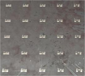
The limitations of modern CMOS technology have created a call to action for novel devices with great scalability potential. Graphene has been recognized as a suitable material for an enhanced transistor channel based on its incredibly large conductivity while also being easily scaled. Previous research has noted the importance of a top gate device structure, which is difficult to accomplish for graphene transistors due to graphene's incompatibility with oxide growth processes. A novel process flow for graphene field effect transistors with scalability is presented. The emphasis is on the growth of multilayer graphene using chemical vapor deposition and the implementation of polydimethylsiloxane as a gate dielectric. Polydimethylsiloxane gate insulator thickness of 815 nm and 570 nm were successfully developed on 4in large-scale wafers. Two devices of similar channel dimensions and different dielectric were compared and mobilities of 14.57cm2V−1s−1 and 0.44 cm2V−1s−1 were measured. Gate voltage sweeps from -20 V to 20 V also demonstrated channel current modulation with a charge neutrality point between 5 V and 8 V, indicating achievement of expected device operation.


 分享
分享

 求助内容:
求助内容: 应助结果提醒方式:
 扫码关注我们
