A. A. Abduvayitov, D. A. Tashmukhamedova, B. E. Umirzakov, A. T. Mamadalimov
{"title":"Effect of Electron Bombardment on the Composition and Structure of CaF2/Si(111) Films","authors":"A. A. Abduvayitov, D. A. Tashmukhamedova, B. E. Umirzakov, A. T. Mamadalimov","doi":"10.1134/S1027451024020228","DOIUrl":null,"url":null,"abstract":"<p>Using the methods of Auger electron spectroscopy, scanning electron microscopy, and measuring the angular dependences of the coefficient of inelastically reflected electrons, changes in the morphology, composition, and structure of CaF<sub>2</sub> surface layers under electron bombardment with an energy of <i>E</i><sub><i>e</i></sub> = 1–8 keV are studied. The composition of the CaF<sub>2</sub> surface changes noticeably at <i>E</i><sub><i>e</i></sub> = 2–3 keV and an electron dose of <i>D</i> ≥ 10<sup>18</sup> cm<sup>–2</sup>. It is found that at a dose of less than 10<sup>18</sup> cm<sup>–2</sup>, electrons are incident on separate sections of the CaF<sub>2</sub> film. As <i>D</i> increases, the sizes of these sections increase, and starting from <i>D</i> = 8 × 10<sup>18</sup> cm<sup>–2</sup>, the boundaries of neighboring sections overlap. The surface is completely covered with Ca atoms. After annealing at 900 K, a single-crystal Ca film is formed. At <i>E</i><sub><i>e</i></sub> = 3 keV, the thickness of the Ca film is ~25–30 Å.</p>","PeriodicalId":671,"journal":{"name":"Journal of Surface Investigation: X-ray, Synchrotron and Neutron Techniques","volume":"18 2","pages":"491 - 494"},"PeriodicalIF":0.4000,"publicationDate":"2024-05-07","publicationTypes":"Journal Article","fieldsOfStudy":null,"isOpenAccess":false,"openAccessPdf":"","citationCount":"0","resultStr":null,"platform":"Semanticscholar","paperid":null,"PeriodicalName":"Journal of Surface Investigation: X-ray, Synchrotron and Neutron Techniques","FirstCategoryId":"1085","ListUrlMain":"https://link.springer.com/article/10.1134/S1027451024020228","RegionNum":0,"RegionCategory":null,"ArticlePicture":[],"TitleCN":null,"AbstractTextCN":null,"PMCID":null,"EPubDate":"","PubModel":"","JCR":"Q4","JCRName":"PHYSICS, CONDENSED MATTER","Score":null,"Total":0}
引用次数: 0
Abstract
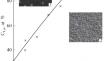
Using the methods of Auger electron spectroscopy, scanning electron microscopy, and measuring the angular dependences of the coefficient of inelastically reflected electrons, changes in the morphology, composition, and structure of CaF2 surface layers under electron bombardment with an energy of Ee = 1–8 keV are studied. The composition of the CaF2 surface changes noticeably at Ee = 2–3 keV and an electron dose of D ≥ 1018 cm–2. It is found that at a dose of less than 1018 cm–2, electrons are incident on separate sections of the CaF2 film. As D increases, the sizes of these sections increase, and starting from D = 8 × 1018 cm–2, the boundaries of neighboring sections overlap. The surface is completely covered with Ca atoms. After annealing at 900 K, a single-crystal Ca film is formed. At Ee = 3 keV, the thickness of the Ca film is ~25–30 Å.
期刊介绍:
Journal of Surface Investigation: X-ray, Synchrotron and Neutron Techniques publishes original articles on the topical problems of solid-state physics, materials science, experimental techniques, condensed media, nanostructures, surfaces of thin films, and phase boundaries: geometric and energetical structures of surfaces, the methods of computer simulations; physical and chemical properties and their changes upon radiation and other treatments; the methods of studies of films and surface layers of crystals (XRD, XPS, synchrotron radiation, neutron and electron diffraction, electron microscopic, scanning tunneling microscopic, atomic force microscopic studies, and other methods that provide data on the surfaces and thin films). Articles related to the methods and technics of structure studies are the focus of the journal. The journal accepts manuscripts of regular articles and reviews in English or Russian language from authors of all countries. All manuscripts are peer-reviewed.


 分享
分享
 求助内容:
求助内容: 应助结果提醒方式:
 扫码关注我们
