Fida Ali, Hyungyu Choi, Nasir Ali, Yasir Hassan, Tien Dat Ngo, Faisal Ahmed, Won-Kyu Park, Zhipei Sun, Won Jong Yoo
{"title":"Achieving Near-Ideal Subthreshold Swing in P-Type WSe2 Field-Effect Transistors","authors":"Fida Ali, Hyungyu Choi, Nasir Ali, Yasir Hassan, Tien Dat Ngo, Faisal Ahmed, Won-Kyu Park, Zhipei Sun, Won Jong Yoo","doi":"10.1002/aelm.202400071","DOIUrl":null,"url":null,"abstract":"<p>The pursuit of near-ideal subthreshold swing (<i>SS</i>) ≈ 60 mV dec<sup>−1</sup> is a primary driving force to realize the power-efficient field-effect transistors (FETs). This challenge is particularly pronounced in 2D material-based FETs, where the presence of a large interface trap density (<i>D<sub>it</sub></i>) imposes limitations on electrostatic control, consequently escalating power consumption. In this study, the gate controllability of 2D FETs is systematically analyzed by fabricating pre-patterned van der Waals (vdW)-contacted p-FETs, varying the WSe<sub>2</sub> channel thickness from monolayer to ten-layer. As a result, the channel thickness is optimized to achieve efficient gate controllability while minimizing <i>D<sub>it</sub></i>. The findings demonstrate negligible hysteresis and excellent subthreshold swing (<i>SS<sub>min</sub></i>) close to the thermal limit (≈60 mV dec<sup>−1</sup>), with a corresponding <i>D<sub>it</sub></i> of ≈10<sup>10</sup> cm<sup>−2</sup> eV<sup>−1</sup>, comparable to <i>D<sub>it</sub></i> values observed in state-of-the-art Si transistors, when utilizing WSe<sub>2</sub> channel thicknesses ≥ five-layer. However, reducing the WSe<sub>2</sub> channel thickness below the trilayer, <i>SS<sub>min</sub></i> (≈91 mV dec<sup>−1</sup>) deviates from the thermal limit, attributed to a comparatively higher <i>D<sub>it</sub></i> (≈10<sup>11</sup> cm<sup>−2</sup> eV<sup>−1</sup>), despite the still lower than values reported for surface-contacted 2D transistors. Furthermore, all devices exhibit consistent p-type characteristics, featuring a high I<sub>ON</sub>/I<sub>OFF</sub> ratio, high mobility, and excellent electrical stability confirmed over several months.</p>","PeriodicalId":110,"journal":{"name":"Advanced Electronic Materials","volume":"10 9","pages":""},"PeriodicalIF":5.3000,"publicationDate":"2024-05-08","publicationTypes":"Journal Article","fieldsOfStudy":null,"isOpenAccess":false,"openAccessPdf":"https://onlinelibrary.wiley.com/doi/epdf/10.1002/aelm.202400071","citationCount":"0","resultStr":null,"platform":"Semanticscholar","paperid":null,"PeriodicalName":"Advanced Electronic Materials","FirstCategoryId":"88","ListUrlMain":"https://advanced.onlinelibrary.wiley.com/doi/10.1002/aelm.202400071","RegionNum":2,"RegionCategory":"材料科学","ArticlePicture":[],"TitleCN":null,"AbstractTextCN":null,"PMCID":null,"EPubDate":"","PubModel":"","JCR":"Q2","JCRName":"MATERIALS SCIENCE, MULTIDISCIPLINARY","Score":null,"Total":0}
引用次数: 0
Abstract
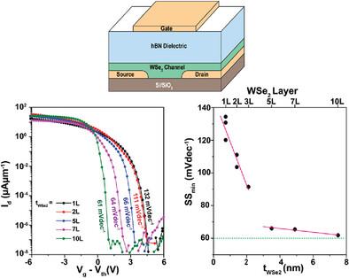
The pursuit of near-ideal subthreshold swing (SS) ≈ 60 mV dec−1 is a primary driving force to realize the power-efficient field-effect transistors (FETs). This challenge is particularly pronounced in 2D material-based FETs, where the presence of a large interface trap density (Dit) imposes limitations on electrostatic control, consequently escalating power consumption. In this study, the gate controllability of 2D FETs is systematically analyzed by fabricating pre-patterned van der Waals (vdW)-contacted p-FETs, varying the WSe2 channel thickness from monolayer to ten-layer. As a result, the channel thickness is optimized to achieve efficient gate controllability while minimizing Dit. The findings demonstrate negligible hysteresis and excellent subthreshold swing (SSmin) close to the thermal limit (≈60 mV dec−1), with a corresponding Dit of ≈1010 cm−2 eV−1, comparable to Dit values observed in state-of-the-art Si transistors, when utilizing WSe2 channel thicknesses ≥ five-layer. However, reducing the WSe2 channel thickness below the trilayer, SSmin (≈91 mV dec−1) deviates from the thermal limit, attributed to a comparatively higher Dit (≈1011 cm−2 eV−1), despite the still lower than values reported for surface-contacted 2D transistors. Furthermore, all devices exhibit consistent p-type characteristics, featuring a high ION/IOFF ratio, high mobility, and excellent electrical stability confirmed over several months.
期刊介绍:
Advanced Electronic Materials is an interdisciplinary forum for peer-reviewed, high-quality, high-impact research in the fields of materials science, physics, and engineering of electronic and magnetic materials. It includes research on physics and physical properties of electronic and magnetic materials, spintronics, electronics, device physics and engineering, micro- and nano-electromechanical systems, and organic electronics, in addition to fundamental research.


 分享
分享
 求助内容:
求助内容: 应助结果提醒方式:
 扫码关注我们
