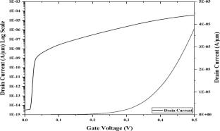
{"title":"Design and Optimization of a Heterojunction (Ge/Si) Vertical-Tunnel Field Effect Transistor (HV-TFET) with a Doped Bar for Low-Power Applications","authors":"Pradeep Kumar Kumawat, Shilpi Birla, Neha Singh","doi":"10.1007/s11664-024-11130-9","DOIUrl":null,"url":null,"abstract":"<div><p>Tunnel field effect transistors (TFETs) are known for lower power requirements than MOSFETs due to their utilization of the band-to-band tunneling mechanism, along with low subthreshold swing (SS). The traditional TFET suffers from low drain current; however, drain current can be improved by modifying the TFET device structure. In this work, a 2-D heterojunction (Ge/Si) vertical-tunnel field effect transistor (HV-TFET) with an optimal design is proposed in which the source region is made of germanium (Ge) due to its low bandgap, while silicon (Si) is used for the regions of drain and channel to mitigate leakage current because of its wider bandgap. The goal of this work is to achieve improved switching by enhancing the ON-state current (<i>I</i><sub>ON</sub>) and reducing the OFF-state current (<i>I</i><sub>OFF</sub>). The currents obtained have values of 1.19 × 10<sup>−3</sup> A/µm and ~ 10<sup>−15</sup> A/µm, respectively, and therefore the <i>I</i><sub>ON</sub>/<i>I</i><sub>OFF</sub> ratio is ~ 10<sup>11</sup> for the device proposed in this paper. Three different dielectric gate oxide materials are used for studying the effect of dielectric materials on the device parameters. Hafnium oxide (HfO<sub>2</sub>) is found to offer the best results when used for gate oxide, and hence is used in the proposed device structure. Also, this work examines a number of electrical parameters of the device structure due to changes in physical device parameters. The results are produced using the Sentaurus TCAD tool to confirm the suitability of the proposed device for use in circuit applications with low-power strategies.</p></div>","PeriodicalId":626,"journal":{"name":"Journal of Electronic Materials","volume":"53 7","pages":"3933 - 3945"},"PeriodicalIF":2.5000,"publicationDate":"2024-05-24","publicationTypes":"Journal Article","fieldsOfStudy":null,"isOpenAccess":false,"openAccessPdf":"","citationCount":"0","resultStr":null,"platform":"Semanticscholar","paperid":null,"PeriodicalName":"Journal of Electronic Materials","FirstCategoryId":"5","ListUrlMain":"https://link.springer.com/article/10.1007/s11664-024-11130-9","RegionNum":4,"RegionCategory":"工程技术","ArticlePicture":[],"TitleCN":null,"AbstractTextCN":null,"PMCID":null,"EPubDate":"","PubModel":"","JCR":"Q3","JCRName":"ENGINEERING, ELECTRICAL & ELECTRONIC","Score":null,"Total":0}
引用次数: 0
Abstract
Tunnel field effect transistors (TFETs) are known for lower power requirements than MOSFETs due to their utilization of the band-to-band tunneling mechanism, along with low subthreshold swing (SS). The traditional TFET suffers from low drain current; however, drain current can be improved by modifying the TFET device structure. In this work, a 2-D heterojunction (Ge/Si) vertical-tunnel field effect transistor (HV-TFET) with an optimal design is proposed in which the source region is made of germanium (Ge) due to its low bandgap, while silicon (Si) is used for the regions of drain and channel to mitigate leakage current because of its wider bandgap. The goal of this work is to achieve improved switching by enhancing the ON-state current (ION) and reducing the OFF-state current (IOFF). The currents obtained have values of 1.19 × 10⁻³ A/µm and ~ 10−15 A/µm, respectively, and therefore the ION/IOFF ratio is ~ 1011 for the device proposed in this paper. Three different dielectric gate oxide materials are used for studying the effect of dielectric materials on the device parameters. Hafnium oxide (HfO2) is found to offer the best results when used for gate oxide, and hence is used in the proposed device structure. Also, this work examines a number of electrical parameters of the device structure due to changes in physical device parameters. The results are produced using the Sentaurus TCAD tool to confirm the suitability of the proposed device for use in circuit applications with low-power strategies.
期刊介绍:
The Journal of Electronic Materials (JEM) reports monthly on the science and technology of electronic materials, while examining new applications for semiconductors, magnetic alloys, dielectrics, nanoscale materials, and photonic materials. The journal welcomes articles on methods for preparing and evaluating the chemical, physical, electronic, and optical properties of these materials. Specific areas of interest are materials for state-of-the-art transistors, nanotechnology, electronic packaging, detectors, emitters, metallization, superconductivity, and energy applications.
Review papers on current topics enable individuals in the field of electronics to keep abreast of activities in areas peripheral to their own. JEM also selects papers from conferences such as the Electronic Materials Conference, the U.S. Workshop on the Physics and Chemistry of II-VI Materials, and the International Conference on Thermoelectrics. It benefits both specialists and non-specialists in the electronic materials field.
A journal of The Minerals, Metals & Materials Society.


 分享
分享
 求助内容:
求助内容: 应助结果提醒方式:
 扫码关注我们
