{"title":"Fabrication of CFETs with Vertically Stacked p-SiGe/n-Si Channels by SiGe/Ge/Si Multilayer Epitaxy and Ge Selective Etching","authors":"Chun-Lin Chu, Szu-Hung Chen, Wei-Yuan Chang, Shu-Han Hsu, Guang-Li Luo* and Wen-Fa Wu, ","doi":"10.1021/acsaelm.4c00411","DOIUrl":null,"url":null,"abstract":"<p >This study presents a straightforward approach for fabricating heterogeneous complementary FET (CFET) devices. The process flow commences with a SiGe/Ge/Si epitaxial multilayer structure grown on a SOI substrate. The source/drains for both stacked devices were straightforwardly performed through P and B implantations with precise depth control, respectively. The isolation of the top p-SiGe FET from the bottom n-Si FET was achieved by etching away the middle Ge sacrificial layer and subsequently filled with SiO<sub>2</sub> dielectric material. The etching selectivity of Ge over Si and Si<sub>0.8</sub>Ge<sub>0.2</sub> by utilizing a H<sub>2</sub>O<sub>2</sub> solution was nearly infinite, resulting in a flawless structure with p-SiGe channels stacked over n-Si channels. Finally, a functional CFET inverter device composed of a top inversion mode (IM) SiGe nanosheet pFET and a bottom IM Si nanosheet nFET was demonstrated.</p>","PeriodicalId":3,"journal":{"name":"ACS Applied Electronic Materials","volume":"6 6","pages":"4304–4310"},"PeriodicalIF":4.7000,"publicationDate":"2024-05-31","publicationTypes":"Journal Article","fieldsOfStudy":null,"isOpenAccess":false,"openAccessPdf":"","citationCount":"0","resultStr":null,"platform":"Semanticscholar","paperid":null,"PeriodicalName":"ACS Applied Electronic Materials","FirstCategoryId":"88","ListUrlMain":"https://pubs.acs.org/doi/10.1021/acsaelm.4c00411","RegionNum":3,"RegionCategory":"材料科学","ArticlePicture":[],"TitleCN":null,"AbstractTextCN":null,"PMCID":null,"EPubDate":"","PubModel":"","JCR":"Q1","JCRName":"ENGINEERING, ELECTRICAL & ELECTRONIC","Score":null,"Total":0}
引用次数: 0
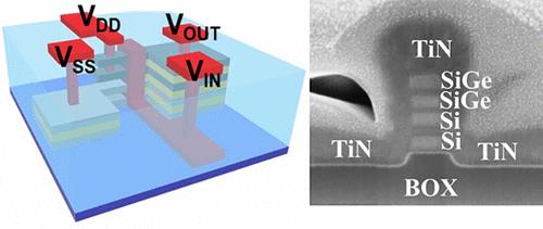
Abstract
This study presents a straightforward approach for fabricating heterogeneous complementary FET (CFET) devices. The process flow commences with a SiGe/Ge/Si epitaxial multilayer structure grown on a SOI substrate. The source/drains for both stacked devices were straightforwardly performed through P and B implantations with precise depth control, respectively. The isolation of the top p-SiGe FET from the bottom n-Si FET was achieved by etching away the middle Ge sacrificial layer and subsequently filled with SiO2 dielectric material. The etching selectivity of Ge over Si and Si0.8Ge0.2 by utilizing a H2O2 solution was nearly infinite, resulting in a flawless structure with p-SiGe channels stacked over n-Si channels. Finally, a functional CFET inverter device composed of a top inversion mode (IM) SiGe nanosheet pFET and a bottom IM Si nanosheet nFET was demonstrated.
通过 SiGe/Ge/Si 多层外延和 Ge 选择性蚀刻技术制造具有垂直堆叠 p-SiGe/n-Si 沟道的 CFET
本研究提出了一种制造异质互补场效应晶体管 (CFET) 器件的直接方法。工艺流程首先是在 SOI 基底面上生长 SiGe/Ge/Si 外延多层结构。两个堆叠器件的源极/漏极分别通过精确控制深度的 P 和 B 植入直接完成。顶部 p-SiGe FET 与底部 n-Si FET 的隔离是通过蚀刻掉中间的 Ge 牺牲层,然后填充二氧化硅介电材料实现的。通过使用 H2O2 溶液,Ge 对 Si 和 Si0.8Ge0.2 的蚀刻选择性几乎为无限大,从而形成了 p-SiGe 沟道堆叠在 n-Si 沟道上的完美结构。最后,展示了一种由顶部反转模式(IM)硅锗纳米片 pFET 和底部 IM 硅纳米片 nFET 组成的功能 CFET 逆变器件。
期刊介绍:
ACS Applied Electronic Materials is an interdisciplinary journal publishing original research covering all aspects of electronic materials. The journal is devoted to reports of new and original experimental and theoretical research of an applied nature that integrate knowledge in the areas of materials science, engineering, optics, physics, and chemistry into important applications of electronic materials. Sample research topics that span the journal's scope are inorganic, organic, ionic and polymeric materials with properties that include conducting, semiconducting, superconducting, insulating, dielectric, magnetic, optoelectronic, piezoelectric, ferroelectric and thermoelectric.
Indexed/Abstracted:
Web of Science SCIE
Scopus
CAS
INSPEC
Portico


 分享
分享
 求助内容:
求助内容: 应助结果提醒方式:
 扫码关注我们
