Rahmat Hadi Saputro, Tatsuro Maeda, Kaoru Toko, Ryo Matsumura* and Naoki Fukata*,
{"title":"High Doping Activation (≥1020 cm–3) in Tensile-Strained n-Ge Alloys Achieved by High-Speed Continuous-Wave Laser Annealing","authors":"Rahmat Hadi Saputro, Tatsuro Maeda, Kaoru Toko, Ryo Matsumura* and Naoki Fukata*, ","doi":"10.1021/acsaelm.4c00399","DOIUrl":null,"url":null,"abstract":"<p >Germanium-based materials are essential for the integration of Group IV optoelectronics in silicon devices. In addition to tensile strain, high n-type doping is critical, as it provides abundant carriers for recombination, potentially enabling higher photoemissions from Ge-based materials. We report here record-high 68% doping activation on n-Ge with ≥10<sup>20</sup> cm<sup>–3</sup> carrier density. This study centers on Sb-doped n-type Ge-on-insulator thin films with Si or Sn alloying grown using high-speed continuous-wave laser annealing (CWLA). Crystal mapping revealed the growth of polycrystalline n-GeSn and n-GeSi thin films with grain sizes up to 4 μm in diameter. Micro-PL measurements showed the PL intensity of n-Ge to be enhanced by the alloying of Sn and Si, with peak intensity 1.5 and 3 times higher for n-GeSn and n-GeSi, respectively. Raman peak red shift and broadening are observed in the samples, indicating high tensile strain and n-type doping. The measured carrier density of CWLA-grown films aligns well with the PL intensity trend, suggesting the process has promise for achieving electrically improved Ge-based thin films.</p>","PeriodicalId":3,"journal":{"name":"ACS Applied Electronic Materials","volume":"6 6","pages":"4297–4303"},"PeriodicalIF":4.7000,"publicationDate":"2024-06-03","publicationTypes":"Journal Article","fieldsOfStudy":null,"isOpenAccess":false,"openAccessPdf":"","citationCount":"0","resultStr":null,"platform":"Semanticscholar","paperid":null,"PeriodicalName":"ACS Applied Electronic Materials","FirstCategoryId":"88","ListUrlMain":"https://pubs.acs.org/doi/10.1021/acsaelm.4c00399","RegionNum":3,"RegionCategory":"材料科学","ArticlePicture":[],"TitleCN":null,"AbstractTextCN":null,"PMCID":null,"EPubDate":"","PubModel":"","JCR":"Q1","JCRName":"ENGINEERING, ELECTRICAL & ELECTRONIC","Score":null,"Total":0}
引用次数: 0
Abstract
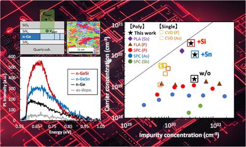
Germanium-based materials are essential for the integration of Group IV optoelectronics in silicon devices. In addition to tensile strain, high n-type doping is critical, as it provides abundant carriers for recombination, potentially enabling higher photoemissions from Ge-based materials. We report here record-high 68% doping activation on n-Ge with ≥1020 cm–3 carrier density. This study centers on Sb-doped n-type Ge-on-insulator thin films with Si or Sn alloying grown using high-speed continuous-wave laser annealing (CWLA). Crystal mapping revealed the growth of polycrystalline n-GeSn and n-GeSi thin films with grain sizes up to 4 μm in diameter. Micro-PL measurements showed the PL intensity of n-Ge to be enhanced by the alloying of Sn and Si, with peak intensity 1.5 and 3 times higher for n-GeSn and n-GeSi, respectively. Raman peak red shift and broadening are observed in the samples, indicating high tensile strain and n-type doping. The measured carrier density of CWLA-grown films aligns well with the PL intensity trend, suggesting the process has promise for achieving electrically improved Ge-based thin films.
期刊介绍:
ACS Applied Electronic Materials is an interdisciplinary journal publishing original research covering all aspects of electronic materials. The journal is devoted to reports of new and original experimental and theoretical research of an applied nature that integrate knowledge in the areas of materials science, engineering, optics, physics, and chemistry into important applications of electronic materials. Sample research topics that span the journal's scope are inorganic, organic, ionic and polymeric materials with properties that include conducting, semiconducting, superconducting, insulating, dielectric, magnetic, optoelectronic, piezoelectric, ferroelectric and thermoelectric.
Indexed/Abstracted:
Web of Science SCIE
Scopus
CAS
INSPEC
Portico


 分享
分享
 求助内容:
求助内容: 应助结果提醒方式:
 扫码关注我们
