Study on plasma-polymerized 1-(trimethylsilyl)pyrrolidine films deposited by plasma-enhanced chemical vapor deposition for use as a Cu diffusion barrier in multilevel metallization process
Chanyong Seo , Namwuk Baek , Shinwon Kang , Gihoon Park , Jihwan Cha , Taesoon Jang , Seonhee Jang , Donggeun Jung
{"title":"Study on plasma-polymerized 1-(trimethylsilyl)pyrrolidine films deposited by plasma-enhanced chemical vapor deposition for use as a Cu diffusion barrier in multilevel metallization process","authors":"Chanyong Seo , Namwuk Baek , Shinwon Kang , Gihoon Park , Jihwan Cha , Taesoon Jang , Seonhee Jang , Donggeun Jung","doi":"10.1016/j.mee.2024.112192","DOIUrl":null,"url":null,"abstract":"<div><p>As integration continues in the modern semiconductor industry, copper (Cu) is used for metal lines and low dielectric constant (low-<em>k</em>) films are used for intermetal dielectrics (IMD) to reduce signal delays occurring in device interconnects. A diffusion barrier is essential between the Cu metal lines and the IMD to prevent Cu diffusion, and silicon carbon-nitride (SiCN) films with relatively low dielectric constants are being widely studied. In this study, SiCN films deposited from 1-(trimethylsilyl)pyrrolidine (TSPD) precursor by plasma-enhanced chemical vapor deposition (PECVD) were investigated for use as a Cu diffusion barrier in multilevel metallization process. This plasma-polymerized TSPD (ppTSPD) monolayer film as SiCN was deposited in plasma powers ranging from 15 to 30 W. The electrical properties of ppTSPD were measured and the chemical properties were analyzed by Fourier-transform infrared spectroscopy (FTIR). The dielectric constant increased with increased plasma power. The lowest dielectric constant of 3.70 and leakage current density at 1 MV/cm of 2.27<span><math><mo>×</mo></math></span>10<sup>−8</sup> A/cm<sup>2</sup> were found for ppTSPD film deposited at 15 W. To verify the Cu diffusion barrier characteristics of the ppTSPD films, a ppTSPD/ppOMCTS bilayer was introduced by using plasma-polymerized octamethylcyclotetrasiloxane (ppOMCTS) as porous low-<em>k</em> SiCOH films. The time-dependent dielectric breakdown (TDDB) characteristic was enhanced around five times than ppOMCTS monolayer used as a reference. The ppTSPD was suggested for fabricating SiCN films for use as a Cu diffusion barrier in multilevel metallization process.</p></div>","PeriodicalId":18557,"journal":{"name":"Microelectronic Engineering","volume":"291 ","pages":"Article 112192"},"PeriodicalIF":3.1000,"publicationDate":"2024-08-01","publicationTypes":"Journal Article","fieldsOfStudy":null,"isOpenAccess":false,"openAccessPdf":"","citationCount":"0","resultStr":null,"platform":"Semanticscholar","paperid":null,"PeriodicalName":"Microelectronic Engineering","FirstCategoryId":"5","ListUrlMain":"https://www.sciencedirect.com/science/article/pii/S0167931724000613","RegionNum":4,"RegionCategory":"工程技术","ArticlePicture":[],"TitleCN":null,"AbstractTextCN":null,"PMCID":null,"EPubDate":"2024/6/8 0:00:00","PubModel":"Epub","JCR":"Q2","JCRName":"ENGINEERING, ELECTRICAL & ELECTRONIC","Score":null,"Total":0}
引用次数: 0
Abstract
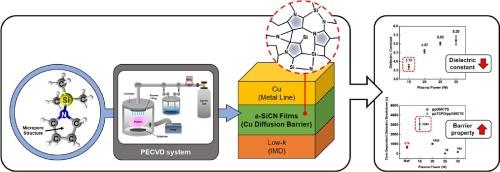
As integration continues in the modern semiconductor industry, copper (Cu) is used for metal lines and low dielectric constant (low-k) films are used for intermetal dielectrics (IMD) to reduce signal delays occurring in device interconnects. A diffusion barrier is essential between the Cu metal lines and the IMD to prevent Cu diffusion, and silicon carbon-nitride (SiCN) films with relatively low dielectric constants are being widely studied. In this study, SiCN films deposited from 1-(trimethylsilyl)pyrrolidine (TSPD) precursor by plasma-enhanced chemical vapor deposition (PECVD) were investigated for use as a Cu diffusion barrier in multilevel metallization process. This plasma-polymerized TSPD (ppTSPD) monolayer film as SiCN was deposited in plasma powers ranging from 15 to 30 W. The electrical properties of ppTSPD were measured and the chemical properties were analyzed by Fourier-transform infrared spectroscopy (FTIR). The dielectric constant increased with increased plasma power. The lowest dielectric constant of 3.70 and leakage current density at 1 MV/cm of 2.2710−8 A/cm2 were found for ppTSPD film deposited at 15 W. To verify the Cu diffusion barrier characteristics of the ppTSPD films, a ppTSPD/ppOMCTS bilayer was introduced by using plasma-polymerized octamethylcyclotetrasiloxane (ppOMCTS) as porous low-k SiCOH films. The time-dependent dielectric breakdown (TDDB) characteristic was enhanced around five times than ppOMCTS monolayer used as a reference. The ppTSPD was suggested for fabricating SiCN films for use as a Cu diffusion barrier in multilevel metallization process.
期刊介绍:
Microelectronic Engineering is the premier nanoprocessing, and nanotechnology journal focusing on fabrication of electronic, photonic, bioelectronic, electromechanic and fluidic devices and systems, and their applications in the broad areas of electronics, photonics, energy, life sciences, and environment. It covers also the expanding interdisciplinary field of "more than Moore" and "beyond Moore" integrated nanoelectronics / photonics and micro-/nano-/bio-systems. Through its unique mixture of peer-reviewed articles, reviews, accelerated publications, short and Technical notes, and the latest research news on key developments, Microelectronic Engineering provides comprehensive coverage of this exciting, interdisciplinary and dynamic new field for researchers in academia and professionals in industry.


 分享
分享
 求助内容:
求助内容: 应助结果提醒方式:
 扫码关注我们
