Aron Michael, Ian Yao-Hsiang Chuang, Chee Yee Kwok, Kazuo Omaki
{"title":"Low-thermal-budget electrically active thick polysilicon for CMOS-First MEMS-last integration.","authors":"Aron Michael, Ian Yao-Hsiang Chuang, Chee Yee Kwok, Kazuo Omaki","doi":"10.1038/s41378-024-00678-5","DOIUrl":null,"url":null,"abstract":"<p><p>Low-thermal-budget, electrically active, and thick polysilicon films are necessary for building a microelectromechanical system (MEMS) on top of a complementary metal oxide semiconductor (CMOS). However, the formation of these polysilicon films is a challenge in this field. Herein, for the first time, the development of in situ phosphorus-doped silicon films deposited under ultrahigh-vacuum conditions (~10<sup>-9</sup> Torr) using electron-beam evaporation (UHVEE) is reported. This process results in electrically active, fully crystallized, low-stress, smooth, and thick polysilicon films with low thermal budgets. The crystallographic, mechanical, and electrical properties of phosphorus-doped UHVEE polysilicon films are studied. These films are compared with intrinsic and boron-doped UHVEE silicon films. Raman spectroscopy, X-ray diffraction (XRD), transmission electron microscopy (TEM) and atomic force microscopy (AFM) are used for crystallographic and surface morphological investigations. Wafer curvature, cantilever deflection profile and resonance frequency measurements are employed to study the mechanical properties of the specimens. Moreover, resistivity measurements are conducted to investigate the electrical properties of the films. Highly vertical, high-aspect-ratio micromachining of UHVEE polysilicon has been developed. A comb-drive structure is designed, simulated, fabricated, and characterized as an actuator and inertial sensor comprising 20-μm-thick in situ phosphorus-doped UHVEE films at a temperature less than 500 °C. The results demonstrate for the first time that UHVEE polysilicon uniquely allows the realization of mechanically and electrically functional MEMS devices with low thermal budgets.</p>","PeriodicalId":18560,"journal":{"name":"Microsystems & Nanoengineering","volume":"10 ","pages":"75"},"PeriodicalIF":9.9000,"publicationDate":"2024-06-06","publicationTypes":"Journal Article","fieldsOfStudy":null,"isOpenAccess":false,"openAccessPdf":"https://www.ncbi.nlm.nih.gov/pmc/articles/PMC11156664/pdf/","citationCount":"0","resultStr":null,"platform":"Semanticscholar","paperid":null,"PeriodicalName":"Microsystems & Nanoengineering","FirstCategoryId":"5","ListUrlMain":"https://doi.org/10.1038/s41378-024-00678-5","RegionNum":1,"RegionCategory":"工程技术","ArticlePicture":[],"TitleCN":null,"AbstractTextCN":null,"PMCID":null,"EPubDate":"2024/1/1 0:00:00","PubModel":"eCollection","JCR":"Q1","JCRName":"INSTRUMENTS & INSTRUMENTATION","Score":null,"Total":0}
引用次数: 0
Abstract
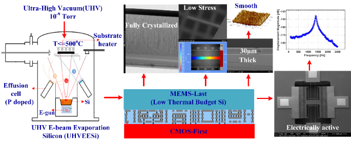
Low-thermal-budget, electrically active, and thick polysilicon films are necessary for building a microelectromechanical system (MEMS) on top of a complementary metal oxide semiconductor (CMOS). However, the formation of these polysilicon films is a challenge in this field. Herein, for the first time, the development of in situ phosphorus-doped silicon films deposited under ultrahigh-vacuum conditions (~10-9 Torr) using electron-beam evaporation (UHVEE) is reported. This process results in electrically active, fully crystallized, low-stress, smooth, and thick polysilicon films with low thermal budgets. The crystallographic, mechanical, and electrical properties of phosphorus-doped UHVEE polysilicon films are studied. These films are compared with intrinsic and boron-doped UHVEE silicon films. Raman spectroscopy, X-ray diffraction (XRD), transmission electron microscopy (TEM) and atomic force microscopy (AFM) are used for crystallographic and surface morphological investigations. Wafer curvature, cantilever deflection profile and resonance frequency measurements are employed to study the mechanical properties of the specimens. Moreover, resistivity measurements are conducted to investigate the electrical properties of the films. Highly vertical, high-aspect-ratio micromachining of UHVEE polysilicon has been developed. A comb-drive structure is designed, simulated, fabricated, and characterized as an actuator and inertial sensor comprising 20-μm-thick in situ phosphorus-doped UHVEE films at a temperature less than 500 °C. The results demonstrate for the first time that UHVEE polysilicon uniquely allows the realization of mechanically and electrically functional MEMS devices with low thermal budgets.
期刊介绍:
Microsystems & Nanoengineering is a comprehensive online journal that focuses on the field of Micro and Nano Electro Mechanical Systems (MEMS and NEMS). It provides a platform for researchers to share their original research findings and review articles in this area. The journal covers a wide range of topics, from fundamental research to practical applications. Published by Springer Nature, in collaboration with the Aerospace Information Research Institute, Chinese Academy of Sciences, and with the support of the State Key Laboratory of Transducer Technology, it is an esteemed publication in the field. As an open access journal, it offers free access to its content, allowing readers from around the world to benefit from the latest developments in MEMS and NEMS.


 分享
分享
 求助内容:
求助内容: 应助结果提醒方式:
 扫码关注我们
