Chi Zhang, Enlong Li, Hongmiao Zhou, Chenhao Xu, Wenwu Li
{"title":"Simulation of 2D ReS2/WSe2 based complementary field-effect transistors towards 1 nm technology node","authors":"Chi Zhang, Enlong Li, Hongmiao Zhou, Chenhao Xu, Wenwu Li","doi":"10.1016/j.mee.2024.112225","DOIUrl":null,"url":null,"abstract":"<div><p>Advanced Integrated Circuit technology demands high-performance channel materials and innovative device architectures to sustain the scaling of field-effect transistors. In this study, we simulate the electrical performance of rhenium disulfide and tungsten diselenide nanosheet FETs (NSFETs) with gate lengths ranging from 12 nm to 8 nm using Technology Computer-Aided Design method. The simulated high performance including 393 μA/μm on-state current and over 10<sup>5</sup> on/off ratio can meet the criteria for integrated circuit applications in the 1 nm technology node. Complementary FET (CFET) simulations are conducted through the vertical stacking of ReS<sub>2</sub> and WSe<sub>2</sub> NSFETs, exhibiting a small parasitic capacitance of 1.0 fF/μm, and notable noise margin (>235 mV) at different process corners. The construction and performance simulation of Static Random-Access Memory (SRAM) is realized through CFET interconnection, involving the calculation of read current and read/write noise margin. This research offers a forward-looking analysis of performance metrics for future 2D materials-based NSFETs, CFETs, and SRAMs.</p></div>","PeriodicalId":18557,"journal":{"name":"Microelectronic Engineering","volume":"292 ","pages":"Article 112225"},"PeriodicalIF":3.1000,"publicationDate":"2024-09-15","publicationTypes":"Journal Article","fieldsOfStudy":null,"isOpenAccess":false,"openAccessPdf":"","citationCount":"0","resultStr":null,"platform":"Semanticscholar","paperid":null,"PeriodicalName":"Microelectronic Engineering","FirstCategoryId":"5","ListUrlMain":"https://www.sciencedirect.com/science/article/pii/S0167931724000947","RegionNum":4,"RegionCategory":"工程技术","ArticlePicture":[],"TitleCN":null,"AbstractTextCN":null,"PMCID":null,"EPubDate":"2024/6/14 0:00:00","PubModel":"Epub","JCR":"Q2","JCRName":"ENGINEERING, ELECTRICAL & ELECTRONIC","Score":null,"Total":0}
引用次数: 0
Abstract
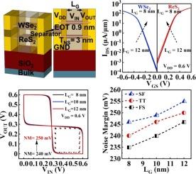
Advanced Integrated Circuit technology demands high-performance channel materials and innovative device architectures to sustain the scaling of field-effect transistors. In this study, we simulate the electrical performance of rhenium disulfide and tungsten diselenide nanosheet FETs (NSFETs) with gate lengths ranging from 12 nm to 8 nm using Technology Computer-Aided Design method. The simulated high performance including 393 μA/μm on-state current and over 105 on/off ratio can meet the criteria for integrated circuit applications in the 1 nm technology node. Complementary FET (CFET) simulations are conducted through the vertical stacking of ReS2 and WSe2 NSFETs, exhibiting a small parasitic capacitance of 1.0 fF/μm, and notable noise margin (>235 mV) at different process corners. The construction and performance simulation of Static Random-Access Memory (SRAM) is realized through CFET interconnection, involving the calculation of read current and read/write noise margin. This research offers a forward-looking analysis of performance metrics for future 2D materials-based NSFETs, CFETs, and SRAMs.
期刊介绍:
Microelectronic Engineering is the premier nanoprocessing, and nanotechnology journal focusing on fabrication of electronic, photonic, bioelectronic, electromechanic and fluidic devices and systems, and their applications in the broad areas of electronics, photonics, energy, life sciences, and environment. It covers also the expanding interdisciplinary field of "more than Moore" and "beyond Moore" integrated nanoelectronics / photonics and micro-/nano-/bio-systems. Through its unique mixture of peer-reviewed articles, reviews, accelerated publications, short and Technical notes, and the latest research news on key developments, Microelectronic Engineering provides comprehensive coverage of this exciting, interdisciplinary and dynamic new field for researchers in academia and professionals in industry.


 分享
分享
 求助内容:
求助内容: 应助结果提醒方式:
 扫码关注我们
