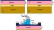
{"title":"Investigating Viability of Split-Stepped Gate Field Plate Design on Ga2O3 MOSFET for High Power Applications","authors":"Priyanshi Goyal, Harsupreet Kaur","doi":"10.1007/s11664-024-11225-3","DOIUrl":null,"url":null,"abstract":"<div><p>A split-stepped gate field plate design has been incorporated on a gallium oxide (Ga<sub>2</sub>O<sub>3</sub>) metal-oxide semiconductor field-effect transistor (MOSFET). The aim of the present work is to unfold the potential of Ga<sub>2</sub>O<sub>3</sub> MOSFET by enhancing its breakdown limits and also to overcome the challenge of simultaneous improvement in power as well as radio frequency (RF) metrics. An extensive simulation study focusing on analog and RF metrics has been carried out using technology computer-aided design simulations of the proposed device in a calibrated environment, and a comparative analysis of split stepped gate field plate design, shorted stepped gate field plate design, and conventional Ga<sub>2</sub>O<sub>3</sub> MOSFET design has also been performed. The results highlight the superiority of the proposed device, and a substantial enhancement in breakdown voltage (i.e., 106.36% relative increase) and power figure-of-merit (i.e., 282.70% relative increase) has been demonstrated.</p></div>","PeriodicalId":626,"journal":{"name":"Journal of Electronic Materials","volume":"53 8","pages":"4544 - 4552"},"PeriodicalIF":2.5000,"publicationDate":"2024-06-08","publicationTypes":"Journal Article","fieldsOfStudy":null,"isOpenAccess":false,"openAccessPdf":"","citationCount":"0","resultStr":null,"platform":"Semanticscholar","paperid":null,"PeriodicalName":"Journal of Electronic Materials","FirstCategoryId":"5","ListUrlMain":"https://link.springer.com/article/10.1007/s11664-024-11225-3","RegionNum":4,"RegionCategory":"工程技术","ArticlePicture":[],"TitleCN":null,"AbstractTextCN":null,"PMCID":null,"EPubDate":"","PubModel":"","JCR":"Q3","JCRName":"ENGINEERING, ELECTRICAL & ELECTRONIC","Score":null,"Total":0}
引用次数: 0
Abstract
A split-stepped gate field plate design has been incorporated on a gallium oxide (Ga2O3) metal-oxide semiconductor field-effect transistor (MOSFET). The aim of the present work is to unfold the potential of Ga2O3 MOSFET by enhancing its breakdown limits and also to overcome the challenge of simultaneous improvement in power as well as radio frequency (RF) metrics. An extensive simulation study focusing on analog and RF metrics has been carried out using technology computer-aided design simulations of the proposed device in a calibrated environment, and a comparative analysis of split stepped gate field plate design, shorted stepped gate field plate design, and conventional Ga2O3 MOSFET design has also been performed. The results highlight the superiority of the proposed device, and a substantial enhancement in breakdown voltage (i.e., 106.36% relative increase) and power figure-of-merit (i.e., 282.70% relative increase) has been demonstrated.
期刊介绍:
The Journal of Electronic Materials (JEM) reports monthly on the science and technology of electronic materials, while examining new applications for semiconductors, magnetic alloys, dielectrics, nanoscale materials, and photonic materials. The journal welcomes articles on methods for preparing and evaluating the chemical, physical, electronic, and optical properties of these materials. Specific areas of interest are materials for state-of-the-art transistors, nanotechnology, electronic packaging, detectors, emitters, metallization, superconductivity, and energy applications.
Review papers on current topics enable individuals in the field of electronics to keep abreast of activities in areas peripheral to their own. JEM also selects papers from conferences such as the Electronic Materials Conference, the U.S. Workshop on the Physics and Chemistry of II-VI Materials, and the International Conference on Thermoelectrics. It benefits both specialists and non-specialists in the electronic materials field.
A journal of The Minerals, Metals & Materials Society.


 分享
分享
 求助内容:
求助内容: 应助结果提醒方式:
 扫码关注我们
