Sicheng Wan, Xiaohua Man, Ping Zhang, Yao Chen, Jinxing He, Zhiyang Luo, Xiaoqing Hu, Yunfei Hu
{"title":"Ultra-Transparent Cerium-Doped Indium Oxide Films Deposited with Industry-Scale Reactive Plasma Deposition","authors":"Sicheng Wan, Xiaohua Man, Ping Zhang, Yao Chen, Jinxing He, Zhiyang Luo, Xiaoqing Hu, Yunfei Hu","doi":"10.1007/s11664-024-11198-3","DOIUrl":null,"url":null,"abstract":"<div><p>Transparent conductive oxide (TCO) films are widely used as electrodes in photovoltaic devices, such as perovskite solar cells and heterojunction solar cells. However, in the conventional physical vapor deposition process, there may be ion bombardment damage to the underlayer coatings, and high deposition temperature also have an adverse effect on perovskite and amorphous silicon layers during TCO deposition. Herein, reactive plasma deposition was effectively utilized for cerium-doped indium oxide (ICO) film as an ultra-transparent electrode. The effects of plasma gun current and the oxygen ratio on the optical and electrical properties, and also on the structure of the ICO films, were investigated. With an industry-scale reactive plasma deposition tool, an outcome of 140-nm ICO film can be achieved within 50 s, which represents a good throughput with the average growth rate of 2.8 nm/s. When the working current was 165 A and the oxygen ratio was 12%, the average transmittance of ICO films reached the highest value (93.09%) in the wavelength range of 400–1200 nm. The average transmittance in the visible wavelength range was 94.23%. The peak transmittance was up to 99.67% at 515 nm, and the corresponding resistivity was 4.68 × 10<sup>−4</sup> Ω cm.</p></div>","PeriodicalId":626,"journal":{"name":"Journal of Electronic Materials","volume":"53 8","pages":"4829 - 4840"},"PeriodicalIF":2.5000,"publicationDate":"2024-06-06","publicationTypes":"Journal Article","fieldsOfStudy":null,"isOpenAccess":false,"openAccessPdf":"","citationCount":"0","resultStr":null,"platform":"Semanticscholar","paperid":null,"PeriodicalName":"Journal of Electronic Materials","FirstCategoryId":"5","ListUrlMain":"https://link.springer.com/article/10.1007/s11664-024-11198-3","RegionNum":4,"RegionCategory":"工程技术","ArticlePicture":[],"TitleCN":null,"AbstractTextCN":null,"PMCID":null,"EPubDate":"","PubModel":"","JCR":"Q3","JCRName":"ENGINEERING, ELECTRICAL & ELECTRONIC","Score":null,"Total":0}
引用次数: 0
Abstract
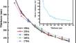
Transparent conductive oxide (TCO) films are widely used as electrodes in photovoltaic devices, such as perovskite solar cells and heterojunction solar cells. However, in the conventional physical vapor deposition process, there may be ion bombardment damage to the underlayer coatings, and high deposition temperature also have an adverse effect on perovskite and amorphous silicon layers during TCO deposition. Herein, reactive plasma deposition was effectively utilized for cerium-doped indium oxide (ICO) film as an ultra-transparent electrode. The effects of plasma gun current and the oxygen ratio on the optical and electrical properties, and also on the structure of the ICO films, were investigated. With an industry-scale reactive plasma deposition tool, an outcome of 140-nm ICO film can be achieved within 50 s, which represents a good throughput with the average growth rate of 2.8 nm/s. When the working current was 165 A and the oxygen ratio was 12%, the average transmittance of ICO films reached the highest value (93.09%) in the wavelength range of 400–1200 nm. The average transmittance in the visible wavelength range was 94.23%. The peak transmittance was up to 99.67% at 515 nm, and the corresponding resistivity was 4.68 × 10⁻⁴ Ω cm.
期刊介绍:
The Journal of Electronic Materials (JEM) reports monthly on the science and technology of electronic materials, while examining new applications for semiconductors, magnetic alloys, dielectrics, nanoscale materials, and photonic materials. The journal welcomes articles on methods for preparing and evaluating the chemical, physical, electronic, and optical properties of these materials. Specific areas of interest are materials for state-of-the-art transistors, nanotechnology, electronic packaging, detectors, emitters, metallization, superconductivity, and energy applications.
Review papers on current topics enable individuals in the field of electronics to keep abreast of activities in areas peripheral to their own. JEM also selects papers from conferences such as the Electronic Materials Conference, the U.S. Workshop on the Physics and Chemistry of II-VI Materials, and the International Conference on Thermoelectrics. It benefits both specialists and non-specialists in the electronic materials field.
A journal of The Minerals, Metals & Materials Society.


 分享
分享
 求助内容:
求助内容: 应助结果提醒方式:
 扫码关注我们
