{"title":"Spintronic device In SWCNT-FET configuration based on chromium oxides thin films consisting of half-metallic ferromagnetic CrO2","authors":"Sudhanshu Dwivedi , Somnath Biswas","doi":"10.1016/j.nanoso.2024.101210","DOIUrl":null,"url":null,"abstract":"<div><p>Spintronic device architectures consisting of ferromagnetic chromium oxide electrodes in single-walled carbon nanotubes field effect transistor (<strong>SWCNT-FET</strong>) configuration have been fabricated to act as strategic building blocks for next generation super-compact high-speed nanoelectronic devices for logic and memory operations. Stable thin films of chromium oxides consisting of half-metallic ferromagnetic chromium-di-oxide (<strong>CrO</strong><sub><strong>2</strong></sub>) were pulsed laser deposited (<strong>PLD</strong>) over lattice-matched rutile-type-tetragonal intermediate <strong>TiO</strong><sub><strong>2</strong></sub> thin layers over thermally oxidized <em><strong>Si</strong></em> substrates for engineering of the spintronic device structure. Focused ion beam (<strong>FIB</strong>) milling was applied to the ferromagnetic chromium oxide thin films for patterning of the source (<em><strong>S</strong></em>) and (<em><strong>D</strong></em>) electrodes. Typical electrical characteristics derived by <strong>ln</strong><em><strong>ρ vs</strong></em>. <strong>T</strong><sup><strong>−1/2</strong></sup> plots confirmed spin-dependent transport (<strong>SDT</strong>) as the dominant mechanism of electrical conduction upto temperatures of ∼280 K along with negative magnetoresistance (<strong>MR</strong>) of ∼30 % at 278 K. Electrical characteristics (output and transfer) of the spintronic device structure were drawn under application of magnetic field (<em><strong>H</strong></em>) in out-of-plane geometry at the temperatures of 5.6 K, 250 K & 300 K. Drain current (<em><strong>I</strong></em><sub><strong>d</strong></sub>) is demonstrated to be controlled effectively as a function of gate bias (<em><strong>V</strong></em><sub><strong>g</strong></sub>) for different fixed <em><strong>V</strong></em><sub><strong>d</strong></sub>-biases at all the device operating temperatures. Change in <strong>%MR</strong> as a function of gate voltage (<em><strong>V</strong></em><sub><strong>g</strong></sub>) was acquired at <em><strong>T</strong></em> = 250 & <em><strong>T</strong></em> = 300 K that displayed higher <strong>%MR</strong> change under out-of-plane geometry of applied field of 0.75 T of the spintronic device operation.</p></div>","PeriodicalId":397,"journal":{"name":"Nano-Structures & Nano-Objects","volume":null,"pages":null},"PeriodicalIF":5.4500,"publicationDate":"2024-06-20","publicationTypes":"Journal Article","fieldsOfStudy":null,"isOpenAccess":false,"openAccessPdf":"","citationCount":"0","resultStr":null,"platform":"Semanticscholar","paperid":null,"PeriodicalName":"Nano-Structures & Nano-Objects","FirstCategoryId":"1","ListUrlMain":"https://www.sciencedirect.com/science/article/pii/S2352507X24001215","RegionNum":0,"RegionCategory":null,"ArticlePicture":[],"TitleCN":null,"AbstractTextCN":null,"PMCID":null,"EPubDate":"","PubModel":"","JCR":"Q1","JCRName":"Physics and Astronomy","Score":null,"Total":0}
引用次数: 0
Abstract
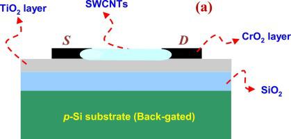
Spintronic device architectures consisting of ferromagnetic chromium oxide electrodes in single-walled carbon nanotubes field effect transistor (SWCNT-FET) configuration have been fabricated to act as strategic building blocks for next generation super-compact high-speed nanoelectronic devices for logic and memory operations. Stable thin films of chromium oxides consisting of half-metallic ferromagnetic chromium-di-oxide (CrO2) were pulsed laser deposited (PLD) over lattice-matched rutile-type-tetragonal intermediate TiO2 thin layers over thermally oxidized Si substrates for engineering of the spintronic device structure. Focused ion beam (FIB) milling was applied to the ferromagnetic chromium oxide thin films for patterning of the source (S) and (D) electrodes. Typical electrical characteristics derived by lnρ vs. T−1/2 plots confirmed spin-dependent transport (SDT) as the dominant mechanism of electrical conduction upto temperatures of ∼280 K along with negative magnetoresistance (MR) of ∼30 % at 278 K. Electrical characteristics (output and transfer) of the spintronic device structure were drawn under application of magnetic field (H) in out-of-plane geometry at the temperatures of 5.6 K, 250 K & 300 K. Drain current (Id) is demonstrated to be controlled effectively as a function of gate bias (Vg) for different fixed Vd-biases at all the device operating temperatures. Change in %MR as a function of gate voltage (Vg) was acquired at T = 250 & T = 300 K that displayed higher %MR change under out-of-plane geometry of applied field of 0.75 T of the spintronic device operation.
由单壁碳纳米管场效应晶体管(SWCNT-FET)配置中的铁磁性氧化铬电极组成的自旋电子器件架构已经制作完成,可作为下一代超紧凑高速纳米电子器件的战略构件,用于逻辑和存储器操作。为了设计自旋电子器件结构,在热氧化硅基底上的晶格匹配金红石型-四方型中间钛氧化物薄层上,用脉冲激光沉积(PLD)了由半金属铁磁性二氧化铬(CrO2)组成的稳定的铬氧化物薄膜。在铁磁性氧化铬薄膜上应用了聚焦离子束(FIB)铣削技术,对源电极(S)和电极(D)进行图案化。通过 lnρ vs. T-1/2 图得出的典型电气特性证实,自旋依赖传输(SDT)是 280 K 以下温度下电气传导的主要机制,278 K 时的负磁阻(MR)为 30%。在 5.6 K、250 K & 和 300 K 的温度下,以平面外几何形状施加磁场(H),绘制了自旋电子器件结构的电气特性(输出和传输)。在所有器件工作温度下,对于不同的固定栅极偏压(Vg),漏极电流(Id)都能得到有效控制。在 T = 250 & T = 300 K 时,获得了栅极电压(Vg)与 MR 百分比变化的函数关系,在自旋电子器件运行的 0.75 T 外加磁场的平面外几何条件下,MR 百分比变化较高。
期刊介绍:
Nano-Structures & Nano-Objects is a new journal devoted to all aspects of the synthesis and the properties of this new flourishing domain. The journal is devoted to novel architectures at the nano-level with an emphasis on new synthesis and characterization methods. The journal is focused on the objects rather than on their applications. However, the research for new applications of original nano-structures & nano-objects in various fields such as nano-electronics, energy conversion, catalysis, drug delivery and nano-medicine is also welcome. The scope of Nano-Structures & Nano-Objects involves: -Metal and alloy nanoparticles with complex nanostructures such as shape control, core-shell and dumbells -Oxide nanoparticles and nanostructures, with complex oxide/metal, oxide/surface and oxide /organic interfaces -Inorganic semi-conducting nanoparticles (quantum dots) with an emphasis on new phases, structures, shapes and complexity -Nanostructures involving molecular inorganic species such as nanoparticles of coordination compounds, molecular magnets, spin transition nanoparticles etc. or organic nano-objects, in particular for molecular electronics -Nanostructured materials such as nano-MOFs and nano-zeolites -Hetero-junctions between molecules and nano-objects, between different nano-objects & nanostructures or between nano-objects & nanostructures and surfaces -Methods of characterization specific of the nano size or adapted for the nano size such as X-ray and neutron scattering, light scattering, NMR, Raman, Plasmonics, near field microscopies, various TEM and SEM techniques, magnetic studies, etc .


 分享
分享
 求助内容:
求助内容: 应助结果提醒方式:
 扫码关注我们
