Yu-Cheng Lu, Jing-Kai Huang, Kai-Yuan Chao, Lain-Jong Li, Vita Pi-Ho Hu
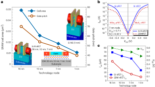
{"title":"Projected performance of Si- and 2D-material-based SRAM circuits ranging from 16 nm to 1 nm technology nodes","authors":"Yu-Cheng Lu, Jing-Kai Huang, Kai-Yuan Chao, Lain-Jong Li, Vita Pi-Ho Hu","doi":"10.1038/s41565-024-01693-3","DOIUrl":null,"url":null,"abstract":"Researchers have been developing 2D materials (2DM) for electronics, which are widely considered a possible replacement for silicon in future technology. Two-dimensional transition metal dichalcogenides are the most promising among the different materials due to their electronic performance and relatively advanced development. Although field-effect transistors (FETs) based on 2D transition metal dichalcogenides have been found to outperform Si in ultrascaled devices, the comparison of 2DM-based and Si-based technologies at the circuit level is still missing. Here we compare 2DM- and Si FET-based static random-access memory (SRAM) circuits across various technology nodes from 16 nm to 1 nm and reveal that the 2DM-based SRAM exhibits superior performance in terms of stability, operating speed and energy efficiency when compared with Si SRAM. This study utilized technology computer-aided design to conduct device and circuit simulations, employing calibrated MoS2 nFETs and WSe2 pFETs. It incorporated layout design rules across various technology nodes to comprehensively analyse their SRAM functionality. The results show that, compared with three-dimensional structure Si transistors at 1 nm node, the planar 2DMFETs exhibited lower capacitance, leading to reduced cell read access time (−16%), reduced time to write (−72%) and lowered dynamic power (−60%). The study highlights the provisional benefits of using planar 2DM transistors to mitigate the performance degradation caused by reduced metal pitch and increased wire resistance in advanced nodes, potentially opening up exciting possibilities for high-performance and low-power circuit applications. Simulations show that two-dimensional-material-based static random-access memory (SRAM) circuits leverage their low parasitic capacitance, counteracting performance declines due to increased interconnect resistance and potentially surpassing Si-based SRAM in terms of both performance and energy efficiency at advanced technology nodes.","PeriodicalId":18915,"journal":{"name":"Nature nanotechnology","volume":"19 7","pages":"1066-1072"},"PeriodicalIF":34.9000,"publicationDate":"2024-06-21","publicationTypes":"Journal Article","fieldsOfStudy":null,"isOpenAccess":false,"openAccessPdf":"","citationCount":"0","resultStr":null,"platform":"Semanticscholar","paperid":null,"PeriodicalName":"Nature nanotechnology","FirstCategoryId":"88","ListUrlMain":"https://www.nature.com/articles/s41565-024-01693-3","RegionNum":1,"RegionCategory":"材料科学","ArticlePicture":[],"TitleCN":null,"AbstractTextCN":null,"PMCID":null,"EPubDate":"","PubModel":"","JCR":"Q1","JCRName":"MATERIALS SCIENCE, MULTIDISCIPLINARY","Score":null,"Total":0}
引用次数: 0
Abstract
Researchers have been developing 2D materials (2DM) for electronics, which are widely considered a possible replacement for silicon in future technology. Two-dimensional transition metal dichalcogenides are the most promising among the different materials due to their electronic performance and relatively advanced development. Although field-effect transistors (FETs) based on 2D transition metal dichalcogenides have been found to outperform Si in ultrascaled devices, the comparison of 2DM-based and Si-based technologies at the circuit level is still missing. Here we compare 2DM- and Si FET-based static random-access memory (SRAM) circuits across various technology nodes from 16 nm to 1 nm and reveal that the 2DM-based SRAM exhibits superior performance in terms of stability, operating speed and energy efficiency when compared with Si SRAM. This study utilized technology computer-aided design to conduct device and circuit simulations, employing calibrated MoS2 nFETs and WSe2 pFETs. It incorporated layout design rules across various technology nodes to comprehensively analyse their SRAM functionality. The results show that, compared with three-dimensional structure Si transistors at 1 nm node, the planar 2DMFETs exhibited lower capacitance, leading to reduced cell read access time (−16%), reduced time to write (−72%) and lowered dynamic power (−60%). The study highlights the provisional benefits of using planar 2DM transistors to mitigate the performance degradation caused by reduced metal pitch and increased wire resistance in advanced nodes, potentially opening up exciting possibilities for high-performance and low-power circuit applications. Simulations show that two-dimensional-material-based static random-access memory (SRAM) circuits leverage their low parasitic capacitance, counteracting performance declines due to increased interconnect resistance and potentially surpassing Si-based SRAM in terms of both performance and energy efficiency at advanced technology nodes.
期刊介绍:
Nature Nanotechnology is a prestigious journal that publishes high-quality papers in various areas of nanoscience and nanotechnology. The journal focuses on the design, characterization, and production of structures, devices, and systems that manipulate and control materials at atomic, molecular, and macromolecular scales. It encompasses both bottom-up and top-down approaches, as well as their combinations.
Furthermore, Nature Nanotechnology fosters the exchange of ideas among researchers from diverse disciplines such as chemistry, physics, material science, biomedical research, engineering, and more. It promotes collaboration at the forefront of this multidisciplinary field. The journal covers a wide range of topics, from fundamental research in physics, chemistry, and biology, including computational work and simulations, to the development of innovative devices and technologies for various industrial sectors such as information technology, medicine, manufacturing, high-performance materials, energy, and environmental technologies. It includes coverage of organic, inorganic, and hybrid materials.


 分享
分享
 求助内容:
求助内容: 应助结果提醒方式:
 扫码关注我们
