Md Akibul Islam, Eric Nicholson, Nima Barri, Momoko Onodera, Danny Starkov, Peter Serles, Shuo He, Boran Kumral, Ali Zavabeti, Haleh Shahsa, Teng Cui, Guorui Wang, Tomoki Machida, C.V. Singh, Tobin Filleter
{"title":"Strain Driven Electrical Bandgap Tuning of Atomically Thin WSe2","authors":"Md Akibul Islam, Eric Nicholson, Nima Barri, Momoko Onodera, Danny Starkov, Peter Serles, Shuo He, Boran Kumral, Ali Zavabeti, Haleh Shahsa, Teng Cui, Guorui Wang, Tomoki Machida, C.V. Singh, Tobin Filleter","doi":"10.1002/aelm.202400225","DOIUrl":null,"url":null,"abstract":"<p>Tuning electrical properties of 2D materials through mechanical strain has predominantly focused on n-type 2D materials like MoS<sub>2</sub> and WS<sub>2</sub>, while p-type 2D materials such as WSe<sub>2</sub> remain relatively unexplored. Here, the impact of controlled mechanical strain on the electron transport characteristics of both mono and bi-layer WSe<sub>2</sub> is studied. Through coupling atomic force microscopy (AFM) nanoindentation techniques and conductive AFM, the ability to finely tune the electronic band structure of WSe<sub>2</sub> is demonstrated. The research offers valuable mechanistic insights into understanding how WSe<sub>2</sub>'s electronic properties respond to mechanical strain, a critical prerequisite for the development of flexible photoelectronic devices. It is also observed that under high pressure, the AFM tip/monolayer WSe<sub>2</sub>/metal substrate junction transitions from Schottky to Ohmic contact, attributed to significant charge injection from the substrate to the WSe<sub>2</sub>. These findings are significant for designing efficient metal/semiconductor contact in thin and flexible PMOS (p-type Metal–Oxide–Semiconductor) devices.</p>","PeriodicalId":110,"journal":{"name":"Advanced Electronic Materials","volume":"10 11","pages":""},"PeriodicalIF":5.3000,"publicationDate":"2024-06-28","publicationTypes":"Journal Article","fieldsOfStudy":null,"isOpenAccess":false,"openAccessPdf":"https://onlinelibrary.wiley.com/doi/epdf/10.1002/aelm.202400225","citationCount":"0","resultStr":null,"platform":"Semanticscholar","paperid":null,"PeriodicalName":"Advanced Electronic Materials","FirstCategoryId":"88","ListUrlMain":"https://advanced.onlinelibrary.wiley.com/doi/10.1002/aelm.202400225","RegionNum":2,"RegionCategory":"材料科学","ArticlePicture":[],"TitleCN":null,"AbstractTextCN":null,"PMCID":null,"EPubDate":"","PubModel":"","JCR":"Q2","JCRName":"MATERIALS SCIENCE, MULTIDISCIPLINARY","Score":null,"Total":0}
引用次数: 0
Abstract
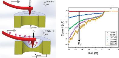
Tuning electrical properties of 2D materials through mechanical strain has predominantly focused on n-type 2D materials like MoS2 and WS2, while p-type 2D materials such as WSe2 remain relatively unexplored. Here, the impact of controlled mechanical strain on the electron transport characteristics of both mono and bi-layer WSe2 is studied. Through coupling atomic force microscopy (AFM) nanoindentation techniques and conductive AFM, the ability to finely tune the electronic band structure of WSe2 is demonstrated. The research offers valuable mechanistic insights into understanding how WSe2's electronic properties respond to mechanical strain, a critical prerequisite for the development of flexible photoelectronic devices. It is also observed that under high pressure, the AFM tip/monolayer WSe2/metal substrate junction transitions from Schottky to Ohmic contact, attributed to significant charge injection from the substrate to the WSe2. These findings are significant for designing efficient metal/semiconductor contact in thin and flexible PMOS (p-type Metal–Oxide–Semiconductor) devices.
期刊介绍:
Advanced Electronic Materials is an interdisciplinary forum for peer-reviewed, high-quality, high-impact research in the fields of materials science, physics, and engineering of electronic and magnetic materials. It includes research on physics and physical properties of electronic and magnetic materials, spintronics, electronics, device physics and engineering, micro- and nano-electromechanical systems, and organic electronics, in addition to fundamental research.


 分享
分享
 求助内容:
求助内容: 应助结果提醒方式:
 扫码关注我们
