Jacopo Pinna, Elisa Pili, Razieh Mehrabi Koushki, Dnyaneshwar S Gavhane, Francesco Carlà, Bart J Kooi, Giuseppe Portale, Maria Antonietta Loi
{"title":"PbI<sub>2</sub> Passivation of Three Dimensional PbS Quantum Dot Superlattices Toward Optoelectronic Metamaterials.","authors":"Jacopo Pinna, Elisa Pili, Razieh Mehrabi Koushki, Dnyaneshwar S Gavhane, Francesco Carlà, Bart J Kooi, Giuseppe Portale, Maria Antonietta Loi","doi":"10.1021/acsnano.4c04076","DOIUrl":null,"url":null,"abstract":"<p><p>Lead chalcogenide colloidal quantum dots are one of the most promising materials to revolutionize the field of short-wavelength infrared optoelectronics due to their bandgap tunability and strong absorption. By self-assembling these quantum dots into ordered superlattices, mobilities approaching those of the bulk counterparts can be achieved while still retaining their original optical properties. The recent literature focused mostly on PbSe-based superlattices, but PbS quantum dots have several advantages, including higher stability. In this work, we demonstrate highly ordered 3D superlattices of PbS quantum dots with tunable thickness up to 200 nm and high coherent ordering, both in-plane and along the thickness. We show that we can successfully exchange the ligands throughout the film without compromising the ordering. The superlattices as the active material of an ion gel-gated field-effect transistor achieve electron mobilities up to 220 cm<sup>2</sup> V<sup>-1</sup> s<sup>-1</sup>. To further improve the device performance, we performed a postdeposition passivation with PbI<sub>2</sub>, which noticeably reduced the subthreshold swing making it reach the Boltzmann limit. We believe this is an important proof of concept showing that it is possible to overcome the problem of high trap densities in quantum dot superlattices enabling their application in optoelectronic devices.</p>","PeriodicalId":21,"journal":{"name":"ACS Nano","volume":" ","pages":"19124-19136"},"PeriodicalIF":16.0000,"publicationDate":"2024-07-23","publicationTypes":"Journal Article","fieldsOfStudy":null,"isOpenAccess":false,"openAccessPdf":"https://www.ncbi.nlm.nih.gov/pmc/articles/PMC11271184/pdf/","citationCount":"0","resultStr":null,"platform":"Semanticscholar","paperid":null,"PeriodicalName":"ACS Nano","FirstCategoryId":"88","ListUrlMain":"https://doi.org/10.1021/acsnano.4c04076","RegionNum":1,"RegionCategory":"材料科学","ArticlePicture":[],"TitleCN":null,"AbstractTextCN":null,"PMCID":null,"EPubDate":"2024/7/2 0:00:00","PubModel":"Epub","JCR":"Q1","JCRName":"CHEMISTRY, MULTIDISCIPLINARY","Score":null,"Total":0}
引用次数: 0
Abstract
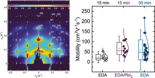
Lead chalcogenide colloidal quantum dots are one of the most promising materials to revolutionize the field of short-wavelength infrared optoelectronics due to their bandgap tunability and strong absorption. By self-assembling these quantum dots into ordered superlattices, mobilities approaching those of the bulk counterparts can be achieved while still retaining their original optical properties. The recent literature focused mostly on PbSe-based superlattices, but PbS quantum dots have several advantages, including higher stability. In this work, we demonstrate highly ordered 3D superlattices of PbS quantum dots with tunable thickness up to 200 nm and high coherent ordering, both in-plane and along the thickness. We show that we can successfully exchange the ligands throughout the film without compromising the ordering. The superlattices as the active material of an ion gel-gated field-effect transistor achieve electron mobilities up to 220 cm2 V-1 s-1. To further improve the device performance, we performed a postdeposition passivation with PbI2, which noticeably reduced the subthreshold swing making it reach the Boltzmann limit. We believe this is an important proof of concept showing that it is possible to overcome the problem of high trap densities in quantum dot superlattices enabling their application in optoelectronic devices.
期刊介绍:
ACS Nano, published monthly, serves as an international forum for comprehensive articles on nanoscience and nanotechnology research at the intersections of chemistry, biology, materials science, physics, and engineering. The journal fosters communication among scientists in these communities, facilitating collaboration, new research opportunities, and advancements through discoveries. ACS Nano covers synthesis, assembly, characterization, theory, and simulation of nanostructures, nanobiotechnology, nanofabrication, methods and tools for nanoscience and nanotechnology, and self- and directed-assembly. Alongside original research articles, it offers thorough reviews, perspectives on cutting-edge research, and discussions envisioning the future of nanoscience and nanotechnology.


 分享
分享
 求助内容:
求助内容: 应助结果提醒方式:
 扫码关注我们
