Heonsu Ahn, Gunho Moon, Hang-gyo Jung, Bingchen Deng, Dong-Hwan Yang, Sera Yang, Cheolhee Han, Hyunje Cho, Youngki Yeo, Cheol-Joo Kim, Chan-Ho Yang, Jonghwan Kim, Si-Young Choi, Hongkun Park, Jongwook Jeon, Jin-Hong Park, Moon-Ho Jo
{"title":"Integrated 1D epitaxial mirror twin boundaries for ultrascaled 2D MoS2 field-effect transistors","authors":"Heonsu Ahn, Gunho Moon, Hang-gyo Jung, Bingchen Deng, Dong-Hwan Yang, Sera Yang, Cheolhee Han, Hyunje Cho, Youngki Yeo, Cheol-Joo Kim, Chan-Ho Yang, Jonghwan Kim, Si-Young Choi, Hongkun Park, Jongwook Jeon, Jin-Hong Park, Moon-Ho Jo","doi":"10.1038/s41565-024-01706-1","DOIUrl":null,"url":null,"abstract":"In atomically thin van der Waals materials, grain boundaries—the line defects between adjacent crystal grains with tilted in-plane rotations—are omnipresent. When the tilting angles are arbitrary, the grain boundaries form inhomogeneous sublattices, giving rise to local electronic states that are not controlled. Here we report on epitaxial realizations of deterministic MoS2 mirror twin boundaries (MTBs) at which two adjoining crystals are reflection mirroring by an exactly 60° rotation by position-controlled epitaxy. We showed that these epitaxial MTBs are one-dimensionally metallic to a circuit length scale. By utilizing the ultimate one-dimensional (1D) feature (width ~0.4 nm and length up to a few tens of micrometres), we incorporated the epitaxial MTBs as a 1D gate to build integrated two-dimensional field-effect transistors (FETs). The critical role of the 1D MTB gate was verified to scale the depletion channel length down to 3.9 nm, resulting in a substantially lowered channel off-current at lower gate voltages. With that, in both individual and array FETs, we demonstrated state-of-the-art performances for low-power logics. The 1D epitaxial MTB gates in this work suggest a novel synthetic pathway for the integration of two-dimensional FETs—that are immune to high gate capacitance—towards ultimate scaling. Mirror twin boundaries in monolayer MoS2—line defects with reflection-mirroring symmetry—are one-dimensionally metallic. In this work, the authors fabricate these mirror twin boundary networks by epitaxity and incorporate them into ultrascaled 2D transistor circuits as gate electrodes.","PeriodicalId":18915,"journal":{"name":"Nature nanotechnology","volume":"19 7","pages":"955-961"},"PeriodicalIF":34.9000,"publicationDate":"2024-07-03","publicationTypes":"Journal Article","fieldsOfStudy":null,"isOpenAccess":false,"openAccessPdf":"","citationCount":"0","resultStr":null,"platform":"Semanticscholar","paperid":null,"PeriodicalName":"Nature nanotechnology","FirstCategoryId":"88","ListUrlMain":"https://www.nature.com/articles/s41565-024-01706-1","RegionNum":1,"RegionCategory":"材料科学","ArticlePicture":[],"TitleCN":null,"AbstractTextCN":null,"PMCID":null,"EPubDate":"","PubModel":"","JCR":"Q1","JCRName":"MATERIALS SCIENCE, MULTIDISCIPLINARY","Score":null,"Total":0}
引用次数: 0
Abstract
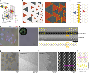
In atomically thin van der Waals materials, grain boundaries—the line defects between adjacent crystal grains with tilted in-plane rotations—are omnipresent. When the tilting angles are arbitrary, the grain boundaries form inhomogeneous sublattices, giving rise to local electronic states that are not controlled. Here we report on epitaxial realizations of deterministic MoS2 mirror twin boundaries (MTBs) at which two adjoining crystals are reflection mirroring by an exactly 60° rotation by position-controlled epitaxy. We showed that these epitaxial MTBs are one-dimensionally metallic to a circuit length scale. By utilizing the ultimate one-dimensional (1D) feature (width ~0.4 nm and length up to a few tens of micrometres), we incorporated the epitaxial MTBs as a 1D gate to build integrated two-dimensional field-effect transistors (FETs). The critical role of the 1D MTB gate was verified to scale the depletion channel length down to 3.9 nm, resulting in a substantially lowered channel off-current at lower gate voltages. With that, in both individual and array FETs, we demonstrated state-of-the-art performances for low-power logics. The 1D epitaxial MTB gates in this work suggest a novel synthetic pathway for the integration of two-dimensional FETs—that are immune to high gate capacitance—towards ultimate scaling. Mirror twin boundaries in monolayer MoS2—line defects with reflection-mirroring symmetry—are one-dimensionally metallic. In this work, the authors fabricate these mirror twin boundary networks by epitaxity and incorporate them into ultrascaled 2D transistor circuits as gate electrodes.
期刊介绍:
Nature Nanotechnology is a prestigious journal that publishes high-quality papers in various areas of nanoscience and nanotechnology. The journal focuses on the design, characterization, and production of structures, devices, and systems that manipulate and control materials at atomic, molecular, and macromolecular scales. It encompasses both bottom-up and top-down approaches, as well as their combinations.
Furthermore, Nature Nanotechnology fosters the exchange of ideas among researchers from diverse disciplines such as chemistry, physics, material science, biomedical research, engineering, and more. It promotes collaboration at the forefront of this multidisciplinary field. The journal covers a wide range of topics, from fundamental research in physics, chemistry, and biology, including computational work and simulations, to the development of innovative devices and technologies for various industrial sectors such as information technology, medicine, manufacturing, high-performance materials, energy, and environmental technologies. It includes coverage of organic, inorganic, and hybrid materials.


 分享
分享
 求助内容:
求助内容: 应助结果提醒方式:
 扫码关注我们
