Chang Lu, Shunhui Zhang, Meili Chen, Haitao Chen, Mengjian Zhu, Zhengwei Zhang, Jun He, Lin Zhang, Xiaoming Yuan
{"title":"Van der Waals epitaxy of type-II band alignment CsPbI3/TMDC heterostructure for optoelectronic applications","authors":"Chang Lu, Shunhui Zhang, Meili Chen, Haitao Chen, Mengjian Zhu, Zhengwei Zhang, Jun He, Lin Zhang, Xiaoming Yuan","doi":"10.1007/s11467-024-1404-9","DOIUrl":null,"url":null,"abstract":"<div><p>Van der Waals epitaxy allows heterostructure formation without considering the lattice match requirement, thus is a promising method to form 2D/2D and 2D/3D heterojunction. Considering the unique optical properties of CsPbI<sub>3</sub> and transition metal dichalcogenides (TMDCs), their heterostructure presents potential applications in both photonics and optoelectronics fields. Here, we demonstrate selective growth of cubic phase CsPbI<sub>3</sub> nanofilm with thickness as thin as 4.0 nm and zigzag/armchair oriented nanowires (NWs) on monolayer WSe<sub>2</sub>. Furthermore, we show growth of CsPbI<sub>3</sub> on both transferred WSe<sub>2</sub> on copper grid and WSe<sub>2</sub>–based optoelectrical devices, providing a platform for structure analysis and device performance modification. Transmission electron microscopy (TEM) results reveal the epitaxial nature of cubic CsPbI<sub>3</sub> phase. The revealed growth fundamental of CsPbI<sub>3</sub> is universal valid for other two-dimensional substrates, offering a great advantage to fabricate CsPbI<sub>3</sub> based van der Waals heterostructures (vdWHs). X-ray photoelectron spectroscopy (XPS) and optical characterization confirm the type-II band alignment, resulting in a fast charge transfer process and the occurrence of a broad emission peak at lower energy. The formation of WSe<sub>2</sub>/CsPbI<sub>3</sub> heterostructure largely enhances the photocurrent from 2.38 nA to 38.59 nA. These findings are vital for bottom-up epitaxy of inorganic semiconductor on atomic thin 2D substrates for optoelectronic applications.</p><div><figure><div><div><picture><source><img></source></picture></div></div></figure></div></div>","PeriodicalId":573,"journal":{"name":"Frontiers of Physics","volume":"19 5","pages":""},"PeriodicalIF":5.3000,"publicationDate":"2024-06-24","publicationTypes":"Journal Article","fieldsOfStudy":null,"isOpenAccess":false,"openAccessPdf":"","citationCount":"0","resultStr":null,"platform":"Semanticscholar","paperid":null,"PeriodicalName":"Frontiers of Physics","FirstCategoryId":"101","ListUrlMain":"https://link.springer.com/article/10.1007/s11467-024-1404-9","RegionNum":2,"RegionCategory":"物理与天体物理","ArticlePicture":[],"TitleCN":null,"AbstractTextCN":null,"PMCID":null,"EPubDate":"","PubModel":"","JCR":"Q1","JCRName":"PHYSICS, MULTIDISCIPLINARY","Score":null,"Total":0}
引用次数: 0
Abstract
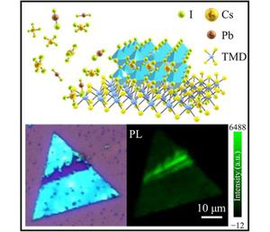
Van der Waals epitaxy allows heterostructure formation without considering the lattice match requirement, thus is a promising method to form 2D/2D and 2D/3D heterojunction. Considering the unique optical properties of CsPbI3 and transition metal dichalcogenides (TMDCs), their heterostructure presents potential applications in both photonics and optoelectronics fields. Here, we demonstrate selective growth of cubic phase CsPbI3 nanofilm with thickness as thin as 4.0 nm and zigzag/armchair oriented nanowires (NWs) on monolayer WSe2. Furthermore, we show growth of CsPbI3 on both transferred WSe2 on copper grid and WSe2–based optoelectrical devices, providing a platform for structure analysis and device performance modification. Transmission electron microscopy (TEM) results reveal the epitaxial nature of cubic CsPbI3 phase. The revealed growth fundamental of CsPbI3 is universal valid for other two-dimensional substrates, offering a great advantage to fabricate CsPbI3 based van der Waals heterostructures (vdWHs). X-ray photoelectron spectroscopy (XPS) and optical characterization confirm the type-II band alignment, resulting in a fast charge transfer process and the occurrence of a broad emission peak at lower energy. The formation of WSe2/CsPbI3 heterostructure largely enhances the photocurrent from 2.38 nA to 38.59 nA. These findings are vital for bottom-up epitaxy of inorganic semiconductor on atomic thin 2D substrates for optoelectronic applications.
期刊介绍:
Frontiers of Physics is an international peer-reviewed journal dedicated to showcasing the latest advancements and significant progress in various research areas within the field of physics. The journal's scope is broad, covering a range of topics that include:
Quantum computation and quantum information
Atomic, molecular, and optical physics
Condensed matter physics, material sciences, and interdisciplinary research
Particle, nuclear physics, astrophysics, and cosmology
The journal's mission is to highlight frontier achievements, hot topics, and cross-disciplinary points in physics, facilitating communication and idea exchange among physicists both in China and internationally. It serves as a platform for researchers to share their findings and insights, fostering collaboration and innovation across different areas of physics.


 分享
分享
 求助内容:
求助内容: 应助结果提醒方式:
 扫码关注我们
