{"title":"Surface Morphology Evolution of MoS2–x by Growth Temperature and Its Effect on Photodetector Properties","authors":"Anibrata Mondal, Y. Ashok Kumar Reddy","doi":"10.1021/acsaelm.4c00665","DOIUrl":null,"url":null,"abstract":"MoS<sub>2</sub>, being an attractive two-dimensional (2-D) material, has gradually become a research hotspot in recent years. Herein, the MoS<sub>2–<i>x</i></sub> thin films are grown through a chemical vapor deposition technique by varying the sulfurization temperature from 700 to 900 °C. X-ray diffraction profile reveals the highly crystalline nature of the sample grown at 800 °C and results in the improved directional orientation of the atoms. A decrement in the intensity of the S 2p peak for the thin film sulfurized at 800 °C signifies the diffusion of the sulfur atoms into the molybdenum atoms, prominently resulting in the development of a nanostructured morphology. The formation of an ohmic contact between the photoactive material and the electrode results in the fast transportation of the charge carriers through the metal-semiconductor interface. The sample grown at 800 °C, achieves a high photocurrent, a sharp rise time, and a superior responsivity of 112.49 μA, 35 ms, and 2.69 A/W, respectively, under the illumination of the visible light (λ = 550 nm) and optical power density of 0.1667 mW/cm<sup>2</sup> attributed to its higher crystalline nature and formation of prominent nanoflake-structured morphology. Finally, with superior figures of merit, the fabricated photodetector signifies its potential for application in optoelectronics devices.","PeriodicalId":3,"journal":{"name":"ACS Applied Electronic Materials","volume":"111 1","pages":""},"PeriodicalIF":4.7000,"publicationDate":"2024-06-23","publicationTypes":"Journal Article","fieldsOfStudy":null,"isOpenAccess":false,"openAccessPdf":"","citationCount":"0","resultStr":null,"platform":"Semanticscholar","paperid":null,"PeriodicalName":"ACS Applied Electronic Materials","FirstCategoryId":"88","ListUrlMain":"https://doi.org/10.1021/acsaelm.4c00665","RegionNum":3,"RegionCategory":"材料科学","ArticlePicture":[],"TitleCN":null,"AbstractTextCN":null,"PMCID":null,"EPubDate":"","PubModel":"","JCR":"Q1","JCRName":"ENGINEERING, ELECTRICAL & ELECTRONIC","Score":null,"Total":0}
引用次数: 0
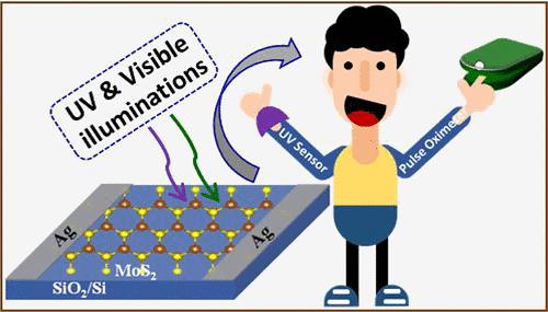
Abstract
MoS2, being an attractive two-dimensional (2-D) material, has gradually become a research hotspot in recent years. Herein, the MoS2–x thin films are grown through a chemical vapor deposition technique by varying the sulfurization temperature from 700 to 900 °C. X-ray diffraction profile reveals the highly crystalline nature of the sample grown at 800 °C and results in the improved directional orientation of the atoms. A decrement in the intensity of the S 2p peak for the thin film sulfurized at 800 °C signifies the diffusion of the sulfur atoms into the molybdenum atoms, prominently resulting in the development of a nanostructured morphology. The formation of an ohmic contact between the photoactive material and the electrode results in the fast transportation of the charge carriers through the metal-semiconductor interface. The sample grown at 800 °C, achieves a high photocurrent, a sharp rise time, and a superior responsivity of 112.49 μA, 35 ms, and 2.69 A/W, respectively, under the illumination of the visible light (λ = 550 nm) and optical power density of 0.1667 mW/cm2 attributed to its higher crystalline nature and formation of prominent nanoflake-structured morphology. Finally, with superior figures of merit, the fabricated photodetector signifies its potential for application in optoelectronics devices.
期刊介绍:
ACS Applied Electronic Materials is an interdisciplinary journal publishing original research covering all aspects of electronic materials. The journal is devoted to reports of new and original experimental and theoretical research of an applied nature that integrate knowledge in the areas of materials science, engineering, optics, physics, and chemistry into important applications of electronic materials. Sample research topics that span the journal's scope are inorganic, organic, ionic and polymeric materials with properties that include conducting, semiconducting, superconducting, insulating, dielectric, magnetic, optoelectronic, piezoelectric, ferroelectric and thermoelectric.
Indexed/Abstracted:
Web of Science SCIE
Scopus
CAS
INSPEC
Portico


 分享
分享
 求助内容:
求助内容: 应助结果提醒方式:
 扫码关注我们
