{"title":"Large-scale growth of MoS2 hybrid layer by chemical vapor deposition with nanosheet promoter","authors":"Jae Hyeok Shin, Hyejin Rhyu, Myung Hyun Kang, Wooseok Song, Sun Sook Lee, Jongsun Lim, Sung Myung","doi":"10.1016/j.mee.2024.112239","DOIUrl":null,"url":null,"abstract":"<div><p>Molybdenum disulfide (MoS<sub>2</sub>) serves as the representative transition metal dichalcogenide material, showing promise for diverse applications owing to its outstanding properties. Extensive research has been conducted on the growth of large-scale MoS<sub>2</sub> films using chemical vapor deposition (CVD) with seeding accelerators for various device applications. In this study, we investigated the growth of large-scale MoS<sub>2</sub> films for potential applications, in which our approach utilized CVD with a homogeneous nanosheet promoter (MoS<sub>2</sub> flakes) and effectively minimized residue creation. Optical and structural analyses confirmed the successful synthesis of a large-scale MoS<sub>2</sub> layer. Moreover, the decoration of metallic nanoparticles on the MoS<sub>2</sub> surface was employed to enhance the functionalities of application devices such as optical sensors and gas sensors. The capability of MoS<sub>2</sub> to act as a nucleation site for nanoparticles during synthesis offered an intriguing pathway for augmenting the attachment and performance of nanoparticles on the MoS<sub>2</sub> surface. The photodetector, integrating a hybrid MoS<sub>2</sub> layer and Cu nanoparticles, exhibited superior photodetection properties, attributed to the increased excitons at the interface between the metal electrodes and MoS<sub>2</sub> films. Furthermore, in order to enhance the characteristics of the gas sensor, Pd nanoparticles were incorporated during the synthesis of MoS<sub>2</sub> layers. This dynamic interface between Pd particles and MoS<sub>2</sub> films presents an opportunity to explore novel materials with enhanced catalytic properties.</p></div>","PeriodicalId":18557,"journal":{"name":"Microelectronic Engineering","volume":"293 ","pages":"Article 112239"},"PeriodicalIF":3.1000,"publicationDate":"2024-07-13","publicationTypes":"Journal Article","fieldsOfStudy":null,"isOpenAccess":false,"openAccessPdf":"https://www.sciencedirect.com/science/article/pii/S0167931724001084/pdfft?md5=49a56c3d40161a07f961c036b291712e&pid=1-s2.0-S0167931724001084-main.pdf","citationCount":"0","resultStr":null,"platform":"Semanticscholar","paperid":null,"PeriodicalName":"Microelectronic Engineering","FirstCategoryId":"5","ListUrlMain":"https://www.sciencedirect.com/science/article/pii/S0167931724001084","RegionNum":4,"RegionCategory":"工程技术","ArticlePicture":[],"TitleCN":null,"AbstractTextCN":null,"PMCID":null,"EPubDate":"","PubModel":"","JCR":"Q2","JCRName":"ENGINEERING, ELECTRICAL & ELECTRONIC","Score":null,"Total":0}
引用次数: 0
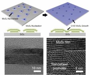
Abstract
Molybdenum disulfide (MoS2) serves as the representative transition metal dichalcogenide material, showing promise for diverse applications owing to its outstanding properties. Extensive research has been conducted on the growth of large-scale MoS2 films using chemical vapor deposition (CVD) with seeding accelerators for various device applications. In this study, we investigated the growth of large-scale MoS2 films for potential applications, in which our approach utilized CVD with a homogeneous nanosheet promoter (MoS2 flakes) and effectively minimized residue creation. Optical and structural analyses confirmed the successful synthesis of a large-scale MoS2 layer. Moreover, the decoration of metallic nanoparticles on the MoS2 surface was employed to enhance the functionalities of application devices such as optical sensors and gas sensors. The capability of MoS2 to act as a nucleation site for nanoparticles during synthesis offered an intriguing pathway for augmenting the attachment and performance of nanoparticles on the MoS2 surface. The photodetector, integrating a hybrid MoS2 layer and Cu nanoparticles, exhibited superior photodetection properties, attributed to the increased excitons at the interface between the metal electrodes and MoS2 films. Furthermore, in order to enhance the characteristics of the gas sensor, Pd nanoparticles were incorporated during the synthesis of MoS2 layers. This dynamic interface between Pd particles and MoS2 films presents an opportunity to explore novel materials with enhanced catalytic properties.
期刊介绍:
Microelectronic Engineering is the premier nanoprocessing, and nanotechnology journal focusing on fabrication of electronic, photonic, bioelectronic, electromechanic and fluidic devices and systems, and their applications in the broad areas of electronics, photonics, energy, life sciences, and environment. It covers also the expanding interdisciplinary field of "more than Moore" and "beyond Moore" integrated nanoelectronics / photonics and micro-/nano-/bio-systems. Through its unique mixture of peer-reviewed articles, reviews, accelerated publications, short and Technical notes, and the latest research news on key developments, Microelectronic Engineering provides comprehensive coverage of this exciting, interdisciplinary and dynamic new field for researchers in academia and professionals in industry.


 分享
分享
 求助内容:
求助内容: 应助结果提醒方式:
 扫码关注我们
