Jordan Pack, Yinjie Guo, Ziyu Liu, Bjarke S. Jessen, Luke Holtzman, Song Liu, Matthew Cothrine, Kenji Watanabe, Takashi Taniguchi, David G. Mandrus, Katayun Barmak, James Hone, Cory R. Dean
{"title":"Charge-transfer contacts for the measurement of correlated states in high-mobility WSe2","authors":"Jordan Pack, Yinjie Guo, Ziyu Liu, Bjarke S. Jessen, Luke Holtzman, Song Liu, Matthew Cothrine, Kenji Watanabe, Takashi Taniguchi, David G. Mandrus, Katayun Barmak, James Hone, Cory R. Dean","doi":"10.1038/s41565-024-01702-5","DOIUrl":null,"url":null,"abstract":"Two-dimensional semiconductors, such as transition metal dichalcogenides, have demonstrated tremendous promise for the development of highly tunable quantum devices. Realizing this potential requires low-resistance electrical contacts that perform well at low temperatures and low densities where quantum properties are relevant. Here we present a new device architecture for two-dimensional semiconductors that utilizes a charge-transfer layer to achieve large hole doping in the contact region, and implement this technique to measure the magnetotransport properties of high-purity monolayer WSe2. We measure a record-high hole mobility of 80,000 cm2 V–1 s–1 and access channel carrier densities as low as 1.6 × 1011 cm−2, an order of magnitude lower than previously achievable. Our ability to realize transparent contact to high-mobility devices at low density enables transport measurements of correlation-driven quantum phases including the observation of a low-temperature metal–insulator transition in a density and temperature regime where Wigner crystal formation is expected and the observation of the fractional quantum Hall effect under large magnetic fields. The charge-transfer contact scheme enables the discovery and manipulation of new quantum phenomena in two-dimensional semiconductors and their heterostructures. By utilizing the van der Waals electron acceptor α-RuCl3, this study establishes a p-type connection with WSe2, facilitating a high hole mobility of 80,000 cm2 V–1 s–1 for investigating quantum transport properties in a magnetic field of over 30 T.","PeriodicalId":18915,"journal":{"name":"Nature nanotechnology","volume":"19 7","pages":"948-954"},"PeriodicalIF":34.9000,"publicationDate":"2024-07-25","publicationTypes":"Journal Article","fieldsOfStudy":null,"isOpenAccess":false,"openAccessPdf":"","citationCount":"0","resultStr":null,"platform":"Semanticscholar","paperid":null,"PeriodicalName":"Nature nanotechnology","FirstCategoryId":"88","ListUrlMain":"https://www.nature.com/articles/s41565-024-01702-5","RegionNum":1,"RegionCategory":"材料科学","ArticlePicture":[],"TitleCN":null,"AbstractTextCN":null,"PMCID":null,"EPubDate":"","PubModel":"","JCR":"Q1","JCRName":"MATERIALS SCIENCE, MULTIDISCIPLINARY","Score":null,"Total":0}
引用次数: 0
Abstract
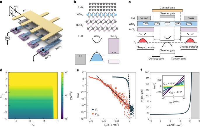
Two-dimensional semiconductors, such as transition metal dichalcogenides, have demonstrated tremendous promise for the development of highly tunable quantum devices. Realizing this potential requires low-resistance electrical contacts that perform well at low temperatures and low densities where quantum properties are relevant. Here we present a new device architecture for two-dimensional semiconductors that utilizes a charge-transfer layer to achieve large hole doping in the contact region, and implement this technique to measure the magnetotransport properties of high-purity monolayer WSe2. We measure a record-high hole mobility of 80,000 cm2 V–1 s–1 and access channel carrier densities as low as 1.6 × 1011 cm−2, an order of magnitude lower than previously achievable. Our ability to realize transparent contact to high-mobility devices at low density enables transport measurements of correlation-driven quantum phases including the observation of a low-temperature metal–insulator transition in a density and temperature regime where Wigner crystal formation is expected and the observation of the fractional quantum Hall effect under large magnetic fields. The charge-transfer contact scheme enables the discovery and manipulation of new quantum phenomena in two-dimensional semiconductors and their heterostructures. By utilizing the van der Waals electron acceptor α-RuCl3, this study establishes a p-type connection with WSe2, facilitating a high hole mobility of 80,000 cm2 V–1 s–1 for investigating quantum transport properties in a magnetic field of over 30 T.
期刊介绍:
Nature Nanotechnology is a prestigious journal that publishes high-quality papers in various areas of nanoscience and nanotechnology. The journal focuses on the design, characterization, and production of structures, devices, and systems that manipulate and control materials at atomic, molecular, and macromolecular scales. It encompasses both bottom-up and top-down approaches, as well as their combinations.
Furthermore, Nature Nanotechnology fosters the exchange of ideas among researchers from diverse disciplines such as chemistry, physics, material science, biomedical research, engineering, and more. It promotes collaboration at the forefront of this multidisciplinary field. The journal covers a wide range of topics, from fundamental research in physics, chemistry, and biology, including computational work and simulations, to the development of innovative devices and technologies for various industrial sectors such as information technology, medicine, manufacturing, high-performance materials, energy, and environmental technologies. It includes coverage of organic, inorganic, and hybrid materials.


 分享
分享
 求助内容:
求助内容: 应助结果提醒方式:
 扫码关注我们
