Paula Mouriño, Laura Mercadé, Miguel Sinusía Lozano, Raquel Resta, Amadeu Griol, Karim Ben Saddik, Enrique Barrigón, Sergio Fernández-Garrido, Basilio Javier García, Alejandro Martínez, Víctor J. Gómez
{"title":"Optomechanical Cavities Based on Epitaxial GaP on Nominally (001)-Oriented Si","authors":"Paula Mouriño, Laura Mercadé, Miguel Sinusía Lozano, Raquel Resta, Amadeu Griol, Karim Ben Saddik, Enrique Barrigón, Sergio Fernández-Garrido, Basilio Javier García, Alejandro Martínez, Víctor J. Gómez","doi":"10.1002/admt.202400525","DOIUrl":null,"url":null,"abstract":"<p>Gallium Phosphide (GaP) has recently received considerable attention as a suitable material for building photonic integrated circuits due to its remarkable optical and piezoelectric properties. Usually, GaP is grown epitaxially on III–V substrates to keep its crystallinity and later transferred to silicon wafers for further processing. Here, an alternative promising route for the fabrication of optomechanical (OM) cavities on GaP epitaxially grown on nominally (001)-oriented Si is introduced by using a two-step process consisting of a low-temperature etching of GaP followed by selective etching of the underneath silicon. The low-temperature (–30 °C) during the dry-etching of GaP hinders the lateral etching rate, preserving the pattern with a deviation between the design and the pattern in the GaP layer lower than 5%, avoiding the complex process of transferring and bonding a GaP wafer to a silicon-on-insulator wafer. To demonstrate the quality and feasibility of the proposed fabrication route, suspended OM cavities are fabricated and experimentally characterized. The cavities exhibit optical quality factors between 10<sup>3</sup> and 10<sup>4</sup> at telecom wavelengths, and localized mechanical resonances ≈3.1 GHz with quality factors ≈63 when measured at room temperature. These results suggest a simple and low-cost way to build GaP-based photonic devices directly integrated on industry-standard Si(001) photonic wafers.</p>","PeriodicalId":7292,"journal":{"name":"Advanced Materials Technologies","volume":"9 24","pages":""},"PeriodicalIF":6.4000,"publicationDate":"2024-07-27","publicationTypes":"Journal Article","fieldsOfStudy":null,"isOpenAccess":false,"openAccessPdf":"https://onlinelibrary.wiley.com/doi/epdf/10.1002/admt.202400525","citationCount":"0","resultStr":null,"platform":"Semanticscholar","paperid":null,"PeriodicalName":"Advanced Materials Technologies","FirstCategoryId":"88","ListUrlMain":"https://advanced.onlinelibrary.wiley.com/doi/10.1002/admt.202400525","RegionNum":3,"RegionCategory":"材料科学","ArticlePicture":[],"TitleCN":null,"AbstractTextCN":null,"PMCID":null,"EPubDate":"","PubModel":"","JCR":"Q1","JCRName":"MATERIALS SCIENCE, MULTIDISCIPLINARY","Score":null,"Total":0}
引用次数: 0
Abstract
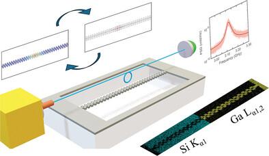
Gallium Phosphide (GaP) has recently received considerable attention as a suitable material for building photonic integrated circuits due to its remarkable optical and piezoelectric properties. Usually, GaP is grown epitaxially on III–V substrates to keep its crystallinity and later transferred to silicon wafers for further processing. Here, an alternative promising route for the fabrication of optomechanical (OM) cavities on GaP epitaxially grown on nominally (001)-oriented Si is introduced by using a two-step process consisting of a low-temperature etching of GaP followed by selective etching of the underneath silicon. The low-temperature (–30 °C) during the dry-etching of GaP hinders the lateral etching rate, preserving the pattern with a deviation between the design and the pattern in the GaP layer lower than 5%, avoiding the complex process of transferring and bonding a GaP wafer to a silicon-on-insulator wafer. To demonstrate the quality and feasibility of the proposed fabrication route, suspended OM cavities are fabricated and experimentally characterized. The cavities exhibit optical quality factors between 103 and 104 at telecom wavelengths, and localized mechanical resonances ≈3.1 GHz with quality factors ≈63 when measured at room temperature. These results suggest a simple and low-cost way to build GaP-based photonic devices directly integrated on industry-standard Si(001) photonic wafers.
磷化镓(GaP)因其卓越的光学和压电特性,最近作为一种适用于构建光子集成电路的材料受到了广泛关注。通常,GaP 是在 III-V 基底上外延生长以保持其结晶性,然后转移到硅晶片上进行进一步加工。本文介绍了在名义(001)取向硅上外延生长的 GaP 上制造光机械(OM)空腔的另一条可行路线,该路线采用两步工艺,包括低温蚀刻 GaP,然后选择性蚀刻下面的硅。GaP 干蚀刻过程中的低温(-30 °C)阻碍了横向蚀刻速度,从而保留了图案,使 GaP 层中设计与图案之间的偏差低于 5%,避免了将 GaP 硅片转移和粘接到硅绝缘体硅片的复杂过程。为了证明所建议的制造路线的质量和可行性,我们制造了悬浮 OM 型腔,并对其进行了实验表征。这些空腔在电信波长下的光学品质因数介于 103 和 104 之间,在室温下测量的局部机械共振频率≈3.1 GHz,品质因数≈63。这些结果表明,在工业标准硅(001)光子晶片上直接集成基于 GaP 的光子器件是一种简单而低成本的方法。
期刊介绍:
Advanced Materials Technologies Advanced Materials Technologies is the new home for all technology-related materials applications research, with particular focus on advanced device design, fabrication and integration, as well as new technologies based on novel materials. It bridges the gap between fundamental laboratory research and industry.


 分享
分享
 求助内容:
求助内容: 应助结果提醒方式:
 扫码关注我们
