Hwanhui Yun, Deyuan Lyu, Yang Lv, Brandon R Zink, Pravin Khanal, Bowei Zhou, Wei-Gang Wang, Jian-Ping Wang, K Andre Mkhoyan
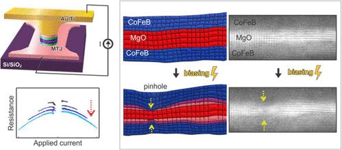
{"title":"Uncovering Atomic Migrations Behind Magnetic Tunnel Junction Breakdown.","authors":"Hwanhui Yun, Deyuan Lyu, Yang Lv, Brandon R Zink, Pravin Khanal, Bowei Zhou, Wei-Gang Wang, Jian-Ping Wang, K Andre Mkhoyan","doi":"10.1021/acsnano.4c08023","DOIUrl":null,"url":null,"abstract":"<p><p>As advances in computing technology increase demand for efficient data storage solutions, spintronic magnetic tunnel junction (MTJ)-based magnetic random-access memory (MRAM) devices emerge as promising alternatives to traditional charge-based memory devices. Successful applications of such spintronic devices necessitate understanding not only their ideal working principles but also their breakdown mechanisms. Employing an in situ electrical biasing system, atomic-resolution scanning transmission electron microscopy (STEM) reveals two distinct breakdown mechanisms. Soft breakdown occurs at relatively low electric currents due to electromigration, wherein restructuring of MTJ core layers forms ultrathin regions in the dielectric MgO layer and edge conducting paths, reducing device resistance. Complete breakdown occurs at relatively high electric currents due to a combination of joule heating and electromigration, melting MTJ component layers at temperatures below their bulk melting points. Time-resolved, atomic-scale STEM studies of functional devices provide insight into the evolution of structure and composition during device operation, serving as an innovative experimental approach for a wide variety of electronic devices.</p>","PeriodicalId":21,"journal":{"name":"ACS Nano","volume":" ","pages":"25708-25715"},"PeriodicalIF":16.0000,"publicationDate":"2024-09-17","publicationTypes":"Journal Article","fieldsOfStudy":null,"isOpenAccess":false,"openAccessPdf":"","citationCount":"0","resultStr":null,"platform":"Semanticscholar","paperid":null,"PeriodicalName":"ACS Nano","FirstCategoryId":"88","ListUrlMain":"https://doi.org/10.1021/acsnano.4c08023","RegionNum":1,"RegionCategory":"材料科学","ArticlePicture":[],"TitleCN":null,"AbstractTextCN":null,"PMCID":null,"EPubDate":"2024/8/20 0:00:00","PubModel":"Epub","JCR":"Q1","JCRName":"CHEMISTRY, MULTIDISCIPLINARY","Score":null,"Total":0}
引用次数: 0
Abstract
As advances in computing technology increase demand for efficient data storage solutions, spintronic magnetic tunnel junction (MTJ)-based magnetic random-access memory (MRAM) devices emerge as promising alternatives to traditional charge-based memory devices. Successful applications of such spintronic devices necessitate understanding not only their ideal working principles but also their breakdown mechanisms. Employing an in situ electrical biasing system, atomic-resolution scanning transmission electron microscopy (STEM) reveals two distinct breakdown mechanisms. Soft breakdown occurs at relatively low electric currents due to electromigration, wherein restructuring of MTJ core layers forms ultrathin regions in the dielectric MgO layer and edge conducting paths, reducing device resistance. Complete breakdown occurs at relatively high electric currents due to a combination of joule heating and electromigration, melting MTJ component layers at temperatures below their bulk melting points. Time-resolved, atomic-scale STEM studies of functional devices provide insight into the evolution of structure and composition during device operation, serving as an innovative experimental approach for a wide variety of electronic devices.
期刊介绍:
ACS Nano, published monthly, serves as an international forum for comprehensive articles on nanoscience and nanotechnology research at the intersections of chemistry, biology, materials science, physics, and engineering. The journal fosters communication among scientists in these communities, facilitating collaboration, new research opportunities, and advancements through discoveries. ACS Nano covers synthesis, assembly, characterization, theory, and simulation of nanostructures, nanobiotechnology, nanofabrication, methods and tools for nanoscience and nanotechnology, and self- and directed-assembly. Alongside original research articles, it offers thorough reviews, perspectives on cutting-edge research, and discussions envisioning the future of nanoscience and nanotechnology.


 分享
分享
 求助内容:
求助内容: 应助结果提醒方式:
 扫码关注我们
