Soh Uenoyama, Kazunori Tanaka, Hiroyasu Fujiwara, Akiyoshi Watanabe, Atsushi Ono
{"title":"Experimental Demonstration of Improvement in Near-Infrared Photodetection Efficiency by Plasmonic Diffraction","authors":"Soh Uenoyama, Kazunori Tanaka, Hiroyasu Fujiwara, Akiyoshi Watanabe, Atsushi Ono","doi":"10.1021/acsaelm.4c01416","DOIUrl":null,"url":null,"abstract":"Near-infrared (NIR) photodetectors are crucial to various applications, including face recognition, night vision, and laser detection and ranging (LiDAR). However, conventional silicon (Si)-based photodetectors exhibit poor sensitivity in the NIR region (λ = 750–1060 nm) because of low photoabsorption within the photoabsorption layer. To overcome this limitation, we proposed a plasmonic diffraction approach that can improve photosensitivity in the NIR regime by properly designing the period of the metal nanograting required to diffract the incident light at large angles in Si, thereby extending the effective propagation length in the photoabsorption layer. In addition, the metal nanograting can transmit the specific wavelength and polarization while enhancing photosensitivity through optimized geometric design. It can be highly advantageous for active sensing applications such as LiDAR, which offers the distinction between signal and noise by selectively transmitting specific wavelengths and polarizations. However, the effectiveness of plasmonic diffraction has never been experimentally demonstrated because it requires the fabrication of a metal nanograting structure with a fine gap. In this study, we successfully fabricated a gold nanograting array on a photodetector and demonstrated a significant improvement (1.79×) in its photosensitivity while employing it as a bandpass filter as well as a polarization filter, even with a single thin gold layer. In addition, providing highly reflective trenches at the border of each pixel will allow the diffracted light to be confined within the pixel, leading to the expansion of image sensors while increasing photosensitivity. This breakthrough will usher in further advances in nanophotonic devices that will enable the development of active sensing technologies with high signal-to-noise ratios.","PeriodicalId":3,"journal":{"name":"ACS Applied Electronic Materials","volume":"24 1","pages":""},"PeriodicalIF":4.7000,"publicationDate":"2024-09-13","publicationTypes":"Journal Article","fieldsOfStudy":null,"isOpenAccess":false,"openAccessPdf":"","citationCount":"0","resultStr":null,"platform":"Semanticscholar","paperid":null,"PeriodicalName":"ACS Applied Electronic Materials","FirstCategoryId":"88","ListUrlMain":"https://doi.org/10.1021/acsaelm.4c01416","RegionNum":3,"RegionCategory":"材料科学","ArticlePicture":[],"TitleCN":null,"AbstractTextCN":null,"PMCID":null,"EPubDate":"","PubModel":"","JCR":"Q1","JCRName":"ENGINEERING, ELECTRICAL & ELECTRONIC","Score":null,"Total":0}
引用次数: 0
Abstract
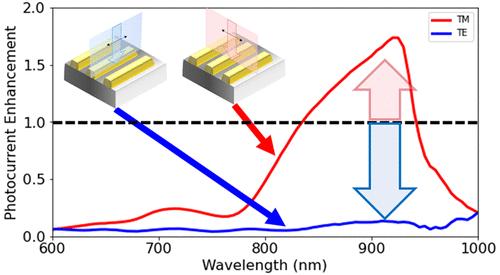
Near-infrared (NIR) photodetectors are crucial to various applications, including face recognition, night vision, and laser detection and ranging (LiDAR). However, conventional silicon (Si)-based photodetectors exhibit poor sensitivity in the NIR region (λ = 750–1060 nm) because of low photoabsorption within the photoabsorption layer. To overcome this limitation, we proposed a plasmonic diffraction approach that can improve photosensitivity in the NIR regime by properly designing the period of the metal nanograting required to diffract the incident light at large angles in Si, thereby extending the effective propagation length in the photoabsorption layer. In addition, the metal nanograting can transmit the specific wavelength and polarization while enhancing photosensitivity through optimized geometric design. It can be highly advantageous for active sensing applications such as LiDAR, which offers the distinction between signal and noise by selectively transmitting specific wavelengths and polarizations. However, the effectiveness of plasmonic diffraction has never been experimentally demonstrated because it requires the fabrication of a metal nanograting structure with a fine gap. In this study, we successfully fabricated a gold nanograting array on a photodetector and demonstrated a significant improvement (1.79×) in its photosensitivity while employing it as a bandpass filter as well as a polarization filter, even with a single thin gold layer. In addition, providing highly reflective trenches at the border of each pixel will allow the diffracted light to be confined within the pixel, leading to the expansion of image sensors while increasing photosensitivity. This breakthrough will usher in further advances in nanophotonic devices that will enable the development of active sensing technologies with high signal-to-noise ratios.
期刊介绍:
ACS Applied Electronic Materials is an interdisciplinary journal publishing original research covering all aspects of electronic materials. The journal is devoted to reports of new and original experimental and theoretical research of an applied nature that integrate knowledge in the areas of materials science, engineering, optics, physics, and chemistry into important applications of electronic materials. Sample research topics that span the journal's scope are inorganic, organic, ionic and polymeric materials with properties that include conducting, semiconducting, superconducting, insulating, dielectric, magnetic, optoelectronic, piezoelectric, ferroelectric and thermoelectric.
Indexed/Abstracted:
Web of Science SCIE
Scopus
CAS
INSPEC
Portico


 分享
分享
 求助内容:
求助内容: 应助结果提醒方式:
 扫码关注我们
